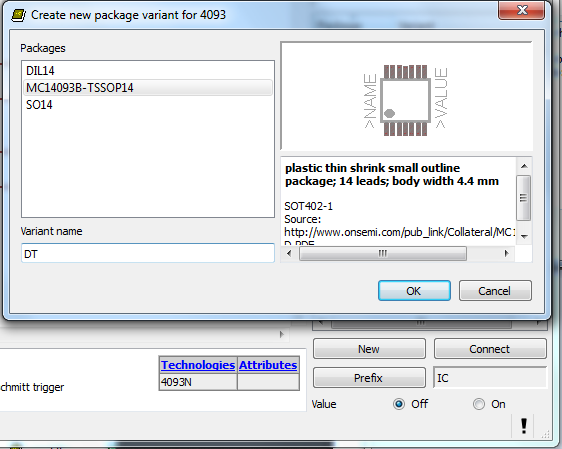
If you’ve spent any time at all laying out your own circuit boards we’re sure you’ve run into the issue of not having the right component or package available in the standard libraries. If it’s a common part, chances are the symbol definition will be there. But perhaps the footprint you want to use is missing? Here’s an easy to follow tutorial which demonstrates how to assign new packages to existing Eagle PCB components. It even shows the basics of how to tweak the footprint to fit your needs (like making SMD footprints easier to hand solder).
This will not teach you how to make your own custom symbols, or how to build packages from scratch. But it will let you locate the package you want to use from a different component, then copy it to your own library for use with different parts. And the techniques shown make this a quick and relatively painless process.
We certainly don’t want to start another comment quagmire like the recent PIC v. AVR discussion. But we’ve used both Kicad and Eagle rather extensively and feel that neither one has really mastered part/footprint creation in a user-friendly way. We like Kicad’s total separation of footprints from components, and it’s myriad of parameters which can be used to tweak the layout. But if you use the same components frequently, Eagle’s standard of linking parts and footprints does end up saving a lot of time. What do you think?


Separating footprints and components is a really stupid idea – same type of package from different manufacturers will have slight differences, thermal requirements will differ etc. Having footprints designed for each device individually give much better results.
Creating new footprint in most good packages takes only couple minutes (especially if you have nice and easy to use wizard like in Altium) and can save lots of trouble.
Try using KiCAD, and you’ll notice that the program is full of stupid. Eagle works like a charm compared to it.
I won’t bother, I have my Altium Designer thanks to our Russian friends.
In my view, this is the biggest problem with open source electronic design tools. You spend a lot of time “filling in the gaps” and not enough time “making your project”.
I looked into KiCad for a project a couple of years ago, and it was useable… except for component libraries. Component library access was non-intuitive, counter productive, and sparsely populated (also poorly documented).
The interface has largely been fixed, but it’s still not at all intuitive or easy to get along with. Nothing as simple as “open a part, make a modification, and save under a new name”. And there is only a smattering of the most common components or outlines in the default library.
Contrast this with AltiumDesigner, which my business partner used for the actual design. The library included all the parts from DigiKey, it lacked for nothing. The parts were cross-referenced by type and description, it was easy to find and drop parts into a schematic.
I spend much of my Kicad time rooting around the footprints library looking for something with the same footprint as the one I want to use (tediously looking at the images one-by-one) because there is no standard naming scheme – no way to tell from the footprint name. For example, look at the footprints beginning with “SOT” and note the associated keywords – frequently there are none. What is the difference between SOT23_5 and SOT23_6? There’s no way to tell without looking at the image, and then on the next project you have to either remember the difference (all of them, for all the footprints) or look again.
Engineers think that writing code is the only important part of a project. They take pains to build a capable engine and infinitely configurable interface, but ignore important aspects. Documentation is usually “put up a wiki and the users will fill it in for us”, or “answer specific questions on StackExchange”. User interface is “we allow the user to configure everything”, with little regard to useability or efficiency.
(How many programs give the users the capability to change the display font size/style/family and fg/bg colors, and how often is this feature needed?)
(How many programs use cryptic glyphs for icons, then use tooltips to interpret the meaning for the user? Would a descriptive word (as glyph/link) eliminate that step and be more efficient?)
Technical writing, user interface design, QA, and artistic merit are all needed to make a good product. A package isn’t just the core software.
^THIS
New version of Kical available 2013-03-19. Kical is well documented but one have to read the docs. It doesn’t enter your brain by magic.
sorry, was to write KiCad…
One has 5 leads, the other has 6. Pretty self explanatory.
I use proteus, I have a hard time finding a footprint for this or that from time to time and have to make my own, not exactly fun, but not too bad. I tried eagle (due to all the supposed library support) and found that it was buggy and crashed a lot so I switched back to proteus (rather expensive though).
erm, just to point out, you could all do this if you read EAGLE’s MANUAL!!!
That’s how I did it
Making symbols and footprints in Eagle is ridiculously easy. Really. I prefer to make all parts myself so I have fool control of the footprint being correct.
Read the manual and/or google for some tutorials and you´ll be going in no time.
fool = full :-p
I recently figured out that by using Eagle’s command line, you can make parts libraries quickly and easily. I wrote an article on the process here: http://codecontainer.org/post/44781560315/creating-parts-in-cadsoft-eagle-fast
Just from using simple photoshop-type apps on my iPhone, I would think it should be possible to design a footprint editor/creator that takes an import of image from datasheet, maybe a few clicks on which areas are which (pins, pads, mask, etc…), and automagically have a precise new device added to your library.
So….which one of you are gonna design that for me? :-)