Few births are easy. Even fewer result in a Nobel Prize, and hardly any at all are the work of three men. This 1965 film from the AT&T archives is a retrospection on the birth of the transistor nine years after its creators, [Walter Brattain], [John Bardeen], and [William Shockley] received a Nobel Prize in Physics for their discovery and implementation of the transistor effect.
The transistor is the result of the study of semiconductors such as germanium. Prior to the research that led directly to the transistor, it was known that the conductivity of semiconductors increases when their temperature is raised. The converse is true for metals such as tungsten. Semiconductor conductivity also increases when they are exposed to light. Another key to their discovery is that when a metal such as copper is in contact with a semiconductor, conductivity is less in one direction than the other. This particular property was exploited in early radio technology as seen in crystal radios, for copper oxide rectifiers used in telephony, and for microwave radar in WWII.
After WWII, AT&T’s Bell Labs put a lot of time and research into the study of semiconductors, as their properties weren’t fully understood. Researchers focused on the simplest semiconductors, silicon and germanium, and did so in two areas: bulk properties and surface properties. During this time, [Shockley] proposed the field effect, supposing that the electrons near the surface of a semiconductor could be controlled under the influence of an external electric field.
This effect would make for great strides in the field of amplification. [Bardeen, Brattain, and Shockley] tested the contact potential of a metal with respect to the surface of a germanium slab. [Brattain] offered that moving the metal conductor across the germanium would produce current flow in a wire connecting the two, and that adding an electrolyte would result in amplification. To experiment, [Bardeen] advocated the model you see below: a piece of germanium with a drop of water for the electrolyte, and a waxed wire penetrating the water to contact the germanium. A second wire makes contact with the water, and both circuits are equipped with a potential.
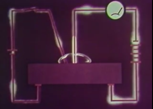
Sure enough, the current on the left influenced the potential through the waxed point, and they had themselves a working semiconductor amplifier. This experiment was vital to the development of the transistor.
The experiment was not without its problems, however. The water electrolyte evaporated too quickly, so they tried glycol borate. That worked much better, but the circuit wouldn’t amplify above 8Hz. They replaced the electrolyte with a thin wafer of gold and used a contact near the edge of the gold instead of the waxed point. [Bardeen, Brattain, and Shockley] dubbed the resulting phenomenon ‘the transistor effect’. Two days before Christmas, 1947, they spoke over the circuit and heard a distinct gain. This arrangement would become the first production line model, known as the point contact transistor.
Further research led to the growth of single crystals of germanium, which made the junction transistor possible. The alloy transistor was developed a few years later, in 1951. These had limited frequency and could only be produced one at a time. In 1954, the diffused base transistor, a high-frequency, high-speed device, was developed.
And this is what was intended all along: an extremely reliable device that could transmit and amplify high-frequency signals at very high speeds and very low power levels. No wonder they won the Nobel Prize.
[Thanks Hernandi]
Retrotechtacular is a weekly column featuring hacks, technology, and kitsch from ages of yore. Help keep it fresh by sending in your ideas for future installments.


Schottky is not on the original patent. He is a grandstander that jumped into the famous picture. He later developed the silicon transistor.
You are mixing up Schottky and Shockley.
Schottky was the first to describe the properties and theory of the metal-semiconductor junction in the 1920ies/1930ies. Schockley was the dude who co-invented the point-contact transistor and invented the junction transitor.
Shockley is further credited with creating the silicon in silicon valley by blatant mismanagment of his company, so his subordinates had to go out and found companies like Fairchield and Intel.
Sorry about that. Had a brain cramp. Schockley name is not on the original patent. There was a long article about him trying to get credit for something he didn’t work on.
Consider too that the point contact and other types of transistors are present in everything we use. From your phone to computer, microwave oven, gaming platform, and vehicle just to name a few.
Now step back for a moment and imagine the transistor had never been invented. It’d be a little like Back to the Future II – in the 1950’s. When the time machine had to use tube for the time circuits. Portable would define anything that weighed ten pounds or more.
Well, point contact transistors were very short lived and never really took off. But you are right that other types of transistors are everywhere.
In my opinion it is not possible to underestimate the importance of the transistor. The transistor gave rise the information age. Together with the Haber-Bosch process it is the most important invention of the 20th century.
TIL about the Haber-Bosch process. Neat stuff, and unlike the transistor, entirely overlooked by my schooling. Kinda weird to realize that most of the food I eat is plants that wouldn’t have grown without industrially produced ammonia fertilizer.
The Germans used the Haber process to manufacture explosives in World War 2 when the selfish British and Americans cut off their supply of Chile saltpeter. Peaceful uses of the process as fertilizer have been catastrophic for the environment too.
>Peaceful uses of the process as fertilizer have been catastrophic for the environment too.
Well, the additional 4 billion people that earth is able to sustain because of artificial nitrogen fixation sure do a lot of damage.
I assume your comment “the selfish British and Americans” was intended to be sarcastic.
Yes indeed – I’d mark the transistor way up there. Consider we’re using a few billion of them to have this exchange.
And yes – the ammonia thing. But that’s a double edged sword as that very same ammonia used in production of illicit drugs.
I can’t say enough good about the book “The Idea Factory: Bell Labs and the Great Age of American Innovation” by Jon Gertner. Fantastic history of Bell Labs, including sections on the transistor and the individuals involved in the patent. It was in my top three favorite books of 2013. I can’t say enough good about it! Gave me a real appreciation for the historical Bell Labs and what they did for modern life in so many ways that we take for granted today. Shameless affiliate plug: http://www.amazon.com/exec/obidos/ASIN/0143122797/bestbookchoices-20
I used to work at Bell Labs, sort of, just after it became AT&T and not “Bell” so much.
Few people realize just how BIG it is. It’s not just one “lab” somewhere, it’s all over the country. New Jersey is a big spot, Atlanta… they have (had) “Bell Labs” all over the place, inventing, building, all kinds of stuff.
The french had submarine transistor cable amplifiers in 1946. Per an article I read in the IEEE times.
Russians were trying to make the FET in the 1920’s.
Blue LED’s to 1908.
>The french had submarine transistor cable amplifiers in 1946. Per an article I read in the IEEE times.
Yes, these were german guys working in France. Herbert Matare and Heinreich Welker. The latter later discovered II-VI semiconductors, possibly coming to your PC in 2015, while being research director at Siemens later on,
>Russians were trying to make the FET in the 1920′s.
Who?
The first credit for FET probably goes to Lilienfeld (not a Russian). His patent from 1924 describes a crude MESFET, though there is no evidence he really made it.
He filed more than one patent on transistors.
> During this time, [Shockley] proposed the field effect, supposing that the electrons near the surface of a semiconductor could be controlled under the influence of an external electric field.
Shockley did not “propose” the field effect. Sure enough, he was researching it, but the original credit for the field effect transistor goes to Julius Edgar Lilienfeld in the 1920ies:
http://en.wikipedia.org/wiki/Julius_Edgar_Lilienfeld
Yes, but Lilienfeld didn’t describe the principles of FET nor did he make a working sample.
Why are you so sure about that? In fact this patent describes a MOSET:
http://worldwide.espacenet.com/textdoc?DB=EPODOC&IDX=US1900018
It is pretty clear from the patent text that he was able to build these devices. In fact, many of the methods he described (reactive PVD,anodic oxidation) are still used today.
The devices may not have been stable enough or had enough gain for real applications.
I DO know this patent. Have you ever tried to make a semiconductor from copper sulphide? Not that it’s not possible – you can make high current schottky diodes and even tunnel diodes. You can make this easily even at home, however it is not easily controllable. The CuS is highly fragile, doesn’t hold on the substrate much and tends to break down at around 6V.
You claimed he did not describe the MOSFET, which he did, without doubt, in this patent.
Apart from Cu2S he also mentioned several other oxidic semiconductors (PbO and some others I don’t remember). It is quite clear that he understood the concept and knew what was required to make it work.
The thing is, of course, that most oxidic and sulphidic semiconductors are horrible channel materials, especially in amorphous form, due to formation of shallow and deep states from structural defects. Even today it is hardly possible to make devices with meaningful transconductance from these materials. CdS is ok, IGZO really is a miracle, but not much else works.
It is possible the Lilienfield built a functional device, but it is quite certain that he did not manage to build a device with characteristics that allow practictal applications.
>The CuS is highly fragile, doesn’t hold on the substrate much and tends to break down at around 6V.
Well, this is wording that would not be used by a semiconductor specialist.
>fragile -> not a property of thin films. Do you mean yield strength?
>hold on substrate -> Do you mean adhesion? Adhesion is significantly influenced by the deposition method. PVD should be fine
>break down voltage -> What do you mean? Break down field of the semiconductor, that gate? 6V is plenty for Vsd. Gate breakdown is not a function of the semiconductor.
Submarine telecommunication cables predate solid state electronics. The repeater amplifiers used high reliability vacuum tubes. Notably those from Western Electric.
I wonder how many people have opened up those metal can transistors when they operate, and noticed a little dim glow of the semiconductor chip in there? Pretty cool really. Still haven’t tried it with the old, large, high power, 2N3055 yet though.
Considering “most” people have never even opened the plastic/metal casing around any electronics, I think you will find that you are in a rather exclusive club (if compared to world population anyways) On HAD however you need to do better than that to be special ;-)
(I should add that I havent opened a transistor while it operated)
Some of my projects with high(ish) power IGBTs have been obliging enough to spontaneously open themselves up and show me a not-so-dim blue-white glow :-)
Ever had a mosfet blow a hole in your perfboard prototype? I have. Left a nice burn spot on my work table too!
I haven’t put a hole through a board, but I have physically ruptured some 1700V/650A modules, opened them up and said ‘well, that gap there is where an IGBT chip used to be.’
Moral of story: when you’re going to higher power electronics it’s essential to have some kind of mechanical debris shield in addition to electrical safety measures.
Check out the scatter shield I put on this
http://img580.imageshack.us/img580/3122/tb6560ahqclose22.jpg
The copper plate on the front of the IC. It has 2 MOSFET bridges in it that have been known to act up. I figured a 16 gauge piece of copper plate should contain the blast. Although it never did blow up on me. That chip is a Toshiba TB6560AHQ stepper motor driver. I built my own stepper motor drivers out of them before the imported assembled drivers were widely available.
In my childhood the transistors I used to get to play with were mostly like these (obsolete by then of course, but still in common use):
http://i.imgur.com/RS3TwCR.jpg
And I opened a lot of them to see something like
http://i.imgur.com/hZ5WZHT.jpg
and to hook them up to an ampermeter head and enjoy some photovoltaic effect. That’s basically all that my lab was limited to. Somehow it was difficult to come by the right values of all parts for any sensible circuit so I don’t remember having built much out of them.
Those MP26Bs served well in low-power audio amplifiers such as those in battery powered radios. Their hfe was larger than 30 and had low Iceo (usually < 0,5 mA), so making amplifiers was fairly easy. These days, I can recommend them for guitar effects (distortions, fuzzes, clippers).
Indeed, I’ve done it with the 2N3055 and a few other TO-3 transistors. Couldn’t ever get it to work with the TO-220 and 92 packages though. It’s pretty nifty, like an orange LED. I didn’t drive it with much current, now I’m curious how bright it could be. If we treated it as an LED, and not a transistor.
i have one and could not open it with small hand tools,
but now that i have a dremel i can not find the darn thing!
i may eventually see for myself if it reeeally IS real!
You can see this phenomenon on KD605 transistor here:
http://www.rayer.g6.cz/elektro/psu4pc/kd605led.jpg
And the page itself, it’s somewhere around half of the page.
http://www.rayer.g6.cz/elektro/psu4pc.htm
Back in 1975, an Army Electronics instructor told us about an “8 Transistor” radio they used to have in the lab (until someone walked off with it). 3 of the transistors were not hooked up to any circuitry, just glued to the circuit board! (Truth in advertising B^)
That is nothing, mine goes to 11.
Upto 2000 transistors… :D
I’ve got a chunk of germanium somewhere, left over from building a radio. I might have a bit of fun and try and see how good a transistor I can make.
I’ve always preferred valves but why not.