[Valentin] recently tipped us about an FPGA development board he just finished. It is called the FleaFPGA and is aimed to get people interested in the world of Field Programmable Gate Arrays. One of the other reasons that also got [Valentin] to design his own board was that he was frustrated with the existing solutions, them being either too pricey or fairly spare in terms of connectivity.
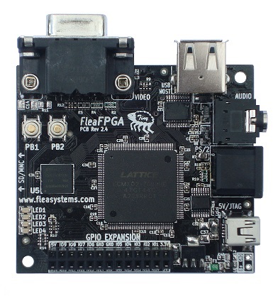
The main components that you can see in the platform shown above are: a lattice MachX02-7000HE FPGA (6864LUTs), 256Mbits of SDRAM, a USB2.0 host port, a 4096-color VGA connector, a 3.5mm stereo connector, an SD/MMC card slot, a PS/2 keyboard/mouse combo port, a few push buttons and LEDs. An expansion header is also present in order to connect the FleaFPGA to future shields that will be developed. Unfortunately only the board schematics have been released and [Valentin] is currently aiming for a price of $60 per board for <100 quantities. You’ll be able to see a video of the board in action after the break, in which the FPGA has been loaded with a 68000 software core running a variation of the Amiga Juggler Demo.


Very nice – I’ll keep watching this development. It could easily become an FPGAduino
I’d really like to have an Altera version of this, not because one is better than another but because that’s what I’m used to. FPGA tools are still in the prehistoric age and switching between vendors is nothing pleasant.
If you don’t already know about them: fpga4fun / knjn.com has a few Altera boards, might suit your fancy
Thanks, my fancy is already suited by DE1 and I’m looking into DE0 Nano, which is slightly more modern. But they are also slightly more expensive than this. I’m also rather curious as to how realistic $60 goal really is.
@Svofski
While I have a healthy respect for Altera, I’ve used Xilinx FPGA tools commercially (albeit schematic capture, not HDL) and Lattice FPGA tools as a hobby, so those are what I am used to – Sorry! :-)
I can assure HaD readers here this production run is well-costed for the 100 boards, assuming I receive anywhere near that number ofc, otherwise (as stated in my production announcement) the cost will be USD$65 plus delivery.
I have, thus far, hand-built six FleaFPGA prototype boards, and shipped four to potential beta-testers who have helped to validate my design.
Regards Valentin
there is crapload of chinese CycloneIII boards on Bay, starting at ~$20, My only problem with them is lack of ram on the same PCB :(
Terasic have a couple of new Altera based dev boards out. One, the P0150, has an Arduino shield socket, a Cyclone V with 77K LEs, a HDMI port, 24 bit audio, 4Gb of LPDDR2 RAM, 4Mb of SRAM, a microSD socket and assorted other connectors. It sells for $180. There’s also a new DE1, the DE1-SOC, which adds 2 ARM A9 cores, an extra 4Gb of SDRAM, 512Mb of SRAM, a couple of USB master ports, 8K more LEs, a gigabit Ethernet port and a few extra IO connectors. On the negative side it loses the Arduino socket and HDMI port (in favour of VGA), but it costs only $20 more (but a $50 academic discount is available).
256Mbits is 32 Megabytes of SDRAM. so I can see where the price justification comes in compared to an arduino.
the other fact being that he’s in Australia. everything in Australia is overpriced. can’t blame him for inflation problems that the country needs to fix themselves money-wise.
The amount of RAM might be an issue if one tried to emulate SNES, but anyway, this device would be a base for one fabulous emulator box.
The size of those SNES carts are in megabits not megabytes! So there is plenty of RAM (256 Mbit).
Wiki: The largest games released (Tales of Phantasia and Star Ocean) contain 48 Mbit of ROM data
It says HSB host mode, but it uses custom chinese piece of crap Mass Storage ONLY controller ch376t, unless he managed to get real documentation out of Chinese company and will be able to implement different usb modes by hand.
true, this looks too good to be true.
there is no word of hid or vcp or whatever other than mass storage.
there is an arduino shield using this chip, and even there it looks like it’s only a file manage and control chip. wtf.
Hello rasz and luke!
My initial thoughts mirrored your own, so naturally I asked for more information from wch-ic.com. What I got back was some demo c code that using the CH376T as a host to enumerate a USB keyboard. Source is written for an 8051 target.
One of the demos I have on my to-do list was to do more than use the high-level mass-storage commands of that chip. However, my HDL skills have only very recently become good enough to even come close to conceivably creating such a demo (learned nearly all of my HDL skills while developing this board! :-), so I apologise for the delay in doing so.
I will now go and post the abovementioned c sources provided to me on my site for anyone who is interested in them.
Regards Valentin
right, looking at the “datasheet” for the fourth time i do actually see a hint on the first page. but i do have to admit the whole ch376 thing seems a bit strange to me. may i ask why you chose this instead of something like a max3421?
cheers
Thanks luke for your reply!
I took a long hard look at the max3421, but pretty much rejected it on price (since FleaFPGA was meant to be strictly a low-cost affair). Nearly gave up on this project altogether when I stumbled upon the CH376T and noticed that very same hint you’re looking at right now etc.. :-)
Regards Valentin
Dont see the code yet
in the mean time found this
http://www.coocox.org/driver_repo/305488dd-734b-4cce-a8a4-39dcfef8cc66/html/hw___c_h376_i_n_c_8h.html
This at least suggest its possible to manipulate buffers inside ch376
>Source is written for an 8051 target
what do you mean by target? those chinese chips (usb memory card readers, pendrive controllers etc) usually have 8051 inside, It sure sounds like they gave you a sample firmware source, if it can enumerate as a HID it could enumerate as anything else, Handling USB inside 8051 in those chips is just swapping numbers between buffers, not much is hardcoded (except buffer sizes).
Companies like Genesyslogic churn out USB pendrive controllers, USB IDE/SATA adapter chips, card readers(for example GL3220), all using same 8051 + DMA engine core.
How much is CH376T? Maxim is ~$8 for well documented and battle tested implementation. Chinese use those stupid clones because they can afford to pay 20 Chinese grad students next to nothing to monkey on keyboards till they stumble by accident on a working piece of code.
$8 worth of BOM is a lot for a small run. You could buy ARM chips with USB OTG these days for a fraction of that and get more functionality out of the deal. Not a pre-made solution, but something worth looking into.
Maxim stuff are nice, but there are lead time issues with their parts.
>>Supports 1.5Mbps low-speed and 12Mbps full-speed, compatible with USB V2.0
oh never mind then, CH376T is USB 1.1
http://www.maximintegrated.com/datasheet/index.mvp/id/3639
>Complies with USB Specification Revision 2.0 (Full-Speed 12Mbps Peripheral, Full-/Low-Speed 12Mbps/1.5Mbps Host)
Same for Maxim part. Not like you can use SPI to handle 480Mbps data rate any time soon.
@rasz
By ‘8051 target’ I mean the demo code is meant to be programmed into a *separate* 8051 microcontroller, which in turn talks to a USB Keyboard via the CH376. Sorry if this isn’t clear.
As for the code to do the above, you may find that here:
http://www.fleasystems.com/source/CH376%20to%20USB%20Keyboard%20demo.7z
The only major gripe I have with wch is that the source code comments are obviously not in English. I’ve been using the 8051 for nearly two decades now and so that wasn’t a deal-breaker for me. YMMV. However, for wider use it would be nice if wch would be kind enough, at the very least, to run their comments through Google translate.. :-)
Cheers.
Just a quick update on this.
I have gone through the vast majority of the vendor-supplied HID demo source code. Deduced enough of the undocumented command set needed to make the CH376 enumerate a USB mouse and read back it’s event data! :-D
More info here:
http://www.fleasystems.com/forums/showthread.php?tid=31
Regards,
Valentin Angelovski
I’d like to see one of these small dev boards that has a HDMI framer or uses LVDS in the FPGA itself to drive the display output to DVI or HDMI. The bigger boards like Digilent ones or the Altera DEn boards do.. but then those boards are too big and expensive to integrate into a finished project. The GPIO looks a little wimpy on this board, I guess most of it is eaten up with the SDRAM… It would be nice to have those signals broken out so you could use them when the SDRAM is deselected.
It’s a 143 MHz SDRAM, so you’d want to avoid adding unnecessary stubs to all the signals.
I have a SoC board with 100MHz+ (I forget what exactly it is) with 2.54mm header breakouts for all of the pins including the SDRAM bus and then DIN 41612 that breaks out all of those signals again for a back plane.. and there is flash memory sharing the data and address bus on the board itself. It seems to work.
It’s not impossible, but it’s making the work for the designer a lot harder, and for very little benefit, because the SDRAM chip would still be attached to the bus, so you wouldn’t be able to use them as general purpose I/O. If you really need more I/O it would make more sense to use a bigger FPGA.
Here you go, all you need to know to connect a HDMI socket to an FPGA
http://www.fpga4fun.com/HDMI.html
Where do I get one? Are they for sale yet?
Hello,
I made an announcement over on my site forums, around doing a small FleaFPGA production run: http://www.fleasystems.com/forums/showthread.php?tid=29&pid=127#pid127
Regards Valentin
Admit it HaD, you waited on posting this until mid-February because it is [Valentin]’s day!
(rimshot!)
LOL yay! :D
I found this at mouser:
http://ca.mouser.com/ProductDetail/Lattice/LCMXO2-7000HE-B-EVN/?qs=DBbQ3l7BldNJuSVNFnSpPw%3d%3d
Same device.
This is a silly question but bear with me because I want to see if I understand this. An FPGA can be used as a disk controller, display controller, cryptographic processor, image recognition engine, whatever I want, based on the software package I install on it, right?
Right, It’s like LEGO, but you get to design the parts ;)
It’s like having a big pile of logic chips in a box that you programmatically wire together at power-up (not sure about the MachXO series but normally this is from an external flash ROM). Anything you can design with that pile of chips (and you’re limited by the number of chips and the propagation time to get signals around the box) you can build. You can implement an entire Amega PC on one, or an arcade console, or a video card etc.
Thanks. Next question: Is writing the code a one time task or can these be reprogrammed?
The FPGA reads in the program (Bit Pattern) from Flash ship when power is applied. To change the programed bit pattern you just re-program the Flash chip. You can also directly input the bit pattern from a PC but that is less useful.
FPGA are reprogrammable. Basically they are based on SRAM designs and thus have to be re-programmed on every power up/reset. This is re-programming can be done via on-chip PROM, on-board EPROM/flash or from a host. Lots of different designs from the vendors and of course their power-on programming abilities come at different costs.
OK. So this leads to my next question: Why aren’t we using these everywhere instead of dedicated CPUs and GPUs? Performance?
Using a TI TIVA processor for the USB could be interesting too since there are lots of examples configuring it as many different classes of device, both host and device. Either use it as a simple bridge or utilize some of the peripherals too?
I feel like one of these days I’m going to need to fab my own board. This is beautiful. I have run out of space with different projects where I needed either more on chip sram (this has a different name depending on who your favorite mfg is), or more logic blocks (also having a different name/makeup per FPGA mfg), so I don’t know about the smallness of this FPGA (which would equal an Altera FPGA of similar LE count).
I’d like to fab my own board with:
1) a 30k LE FPGA
2) an sdram of similar size to this with a 32 bit bus
3) an actual RAMDAC for the VGA out. they’re super cheap and can give you 10 bits per channel easily.
4) everything else brought out to GPIO – not using some high speed riser connect, but a bunch of standard 1mm space pins.
The onboard JTAG programmer exposed via USB is a nice touch.
You might want to look into putting in a SODIMM connector so you can play with different memory sizes or use that for an I/O card when you don’t need memory.
> standard 1mm space pins
Not sure if 1mm space connectors are “standard”. 0.1″ or 2mm pitch ones are more common.
1) 30K gate is small now. I just received a Papilio one which has 500K gates. If you mean 30Kbytes then that’s about the range of some FPGA’s.
2) A 32 Bit Bus is a few GPIO’s but still ok.
3) Most FPGA’s have dual ported ram internally so there great for VGA internally. 10 Bit’s per colour is more than the average eye can see. An 8 Bit per colour R / 2R DAC is as much as you should need.
4) Most of the development boards have 0.1″ spaced headers.
I think you’re a little confused, at least on some parts. :)
1) Gates are not logic cells(Xilinx)/logic elements(Altera)! For comparison, the Xilinx XC3S500E which the Papilio 500k uses, is 10,476 logic cells.
2) A 32 bit bus for _memory_ is pretty big for a dev kit – by standard for most affordable Altera and Xilinx kits they have a 16 bit bus. This makes doing anything tricky when you need to store 32 bit words. Faster memories that have 64 bit bus are available, but more difficult to use. This 32 bit bus would only be for the memory, not for the GPIO that is brought out.
3) FPGAs don’t have enough BRAM internally to do VGA with any decent bit depth or resolution. For example, on the FPGA you were talking about, you have a maximum possible memory usage (you never get this) of 54k. You’d need 900k to do a framebuffer for 640x480x24bpp.
4) You’re right about the pin spacing, I was groggy when I wrote this.
I have just stared learning VHDL but my FPGA has not arrived yet so I am just reading up before it gets here.
I had a lot of trouble choosing something to get started with because a lot of products don’t offer information that is important to my decision.
The things I need to know are –
How much is the basic platform.
How much more do I need to pay for extra stuff like programming interfaces.
How easy is it to use the software.
How much quality documentation is there for beginners.
While cost is a consideration it is by far the least important of the above parameters.
Seriously something with 20 logic cells, easy to use software and quality documentation targeted for beginners would be a thousand times better than something with 500,000 logic cells, pain in the ass software and poor documentation.
If the object is to learn VHDL then any hardware will do. Look at the success of the Arduino platform. A sh.tty little 20 Mips 8 Bit micro-controller, an IDE that is so simple that it’s hard to get things wrong and documentation everywhere.
If you are going to learn something new then the most important aspect is the quality of the documentation.
I have a STM32F104 (micro-controller) development board here that will eventually end up in the bin without ever running a line of code. It is an excellent board with everything I wanted but the software is a nightmare and the documentation was translated from Portuguese or in some cases still in Portuguese. I haven’t been able to even load in the bootloader.
I have a xilinx Spartan 3E – 200K board that I gave up on. This is not a great loss as it has another purpose for which I use it. Once again the let down was the documentation.
Now I am not commenting on the product in this article on HAD as I didn’t look into it. I have already ordered what seemed best at the time.
Having learnt my lesson I started looking for good documentation with no consideration to the hardware.
I ended up buying a papilio one 500K and logic start mega wing because it intended for beginners and seemed to have the best supporting documentation. It’s based in the xilinx Spartan 3E 500,000.
The xilinx software is a nightmare but the documentation goes some way to compensate for this. I am really hoping there is some software out there that is much easier to drive. Perhaps I will end up writing a GUI front end to run a open source tool chain some time later.
What I really would love to hear from this forum is what might be better than what I have especially the software side.
Thanks.
There are 3rd party *pay* frontend tools that are sort of works like “IDE”, but that’s as far as they would go. You pretty much at the mercy of the FPGA/CPLD vendor’s software as the fitting/routing/bit stream generation are propriety and there are *no* open source alternatives for any current parts. Get used to it as *everyone* else has to do that.
The big 3 CPLD/FPGA vendors offer lite versions of their software for free which for practical purpose would handle devices that an average person can afford.
@Rob
Thanks for your questions. Here are my answers :-)
The things I need to know are –
“How much is the basic platform”
Depending on the number of people interested in my project – FleaFPGA will be either USD$65 or USD$60 depending on whether we reach our goal of 100 boards (or even close) or not.
“How much more do I need to pay for extra stuff like programming interfaces.”
USB Type A to Mini B Male adapter cable minimum – that’s it! :-)
Note: ~ $5 USB Hub is recommended only if you need to update the FleaFPGA’s Flash ROM area often (which isn’t recommended anyway – you should be programming the FPGA’s config SRAM instead during testing and development because that doesn’t wear out ;-)
“How easy is it to use the software?”
Lattice Diamond was actually something of a pleasant surprise for this enthusiast, who didn’t really know much about HDL himself 12 months ago.. :-) Quite easy to use, particularly with VHDL (my opinion).
“How much quality documentation is there for beginners.”
Plenty of good user guides around – several are recommended on our site:
http://www.fleasystems.com/fleaFPGA.html#footer
Hope this helps :-)
Regards Valentin
Very cool project, maybe a KickStarter project to get a 100+ orders to hit you BOM cost projection? (FPGAs are on my learning list after I get past a bare-metal ARM +CPDL project… )….
Now, of course, while FPGAs are ‘old-school’ already for BitCoin mining, any idea of the Hashs per Hour you can get from a MachX02-7000HE (mid-range component from Lattice?)
Assuming you can manage to convert the VHDL, and given that a Spartan 3E 500 is just about big enough to run a mining app you should be able to about match that, so about 1 to 1.5Mhash/sec