[nitro2k01] got his hands on a Game Fighter, a clone of the original Game Boy. While there’s a ton of information about the boot ROM and operation of the original Game Boy, not much is known about these clones. [nitro2k01] wanted to learn more, so he used a clock-glitching technique to dump the device’s ROM and made some interesting discoveries about its copyright protection and boot process along the way.
Reading the contents of the Game Boy ROM is a bit challenging. The ROM is readable while booting, but afterwards the address space of the ROM is remapped for interrupt vectors and other uses. There are a couple of methods to get around this, but the simplest method involves glitching the crystal by grounding one of its leads. This causes the CPU to jump to random locations in memory. Eventually the CPU will jump to a location where the boot ROM is accessible (if you’re lucky!).
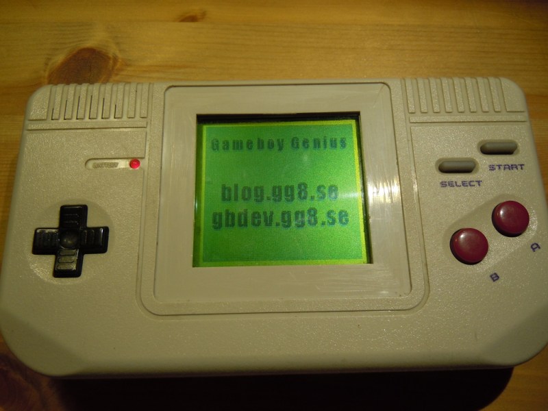
Although [nitro2k01]’s clone can run the same games as the Game Boy, it has a different boot ROM and also has some significant hardware differences. [nitro2k01] managed to use a modified version of the crystal-grounding technique to glitch his clock and dump the clone’s boot ROM. He found that the clone uses an unusual variation on the Game Boy’s copyright-checking technique, along with some other oddities. [nitro2k01] also posted a disassembly of the boot ROM, which he explains in detail.
Thanks for the tip, [Ove].


Very cool. Not sure why people would really care to dumb it, after knowing that all you need is to fake the logo plus set up some hardware to get it to work.
Any game ROM that will pass on the original thing will pass on this one. There are two reasons I did it.
1) “Completionism”. Wanting to know everything there is to know.
2) Getting clues about who made the clone for historic documentation. So far, there have been no visible clues on the board or imprints in the shell as to who’s responsible. Ideally, I would have found a string like “1995 SACHEN” in the boot ROM. (Sachen is a known pirate game company.) Instead I found the half logo which is some kind of clue, but it remains a mystery. I might consider getting in contact with someone to get chip decapped next to look for manufacturer markings, but that would destroy the CPU chip, whereas this method was non-invasive and easy to do, so why not…
I’ve been looking for one of these very clones forever! I think they actually look better than the original gameboy
It looks nice, but usability-wise it leaves a lot to be desired. The distance between the buttons and the circuit board is longer than on a real DMG (the product model of the original Gameboy) which makes the button response suboptimal. The D-pad pivot around a center point just like in the original, but the longer depth makes it feel squishy. The A and B buttons also feel much looser. Whereas the select/start group requires pushing pretty hard to register, as the rubber button pad is flexible and absorbs some of the force. Furthermore, the sound is crappy, owing to a badly designed amplifier. And the LCD screen flickers badly.
If I was more of a heretic, or if I would land another one of these puppies so I have a spare, I might consider modding the internals and put a real DMG screen and buttons in it to resolve the problems I mentioned and make it both good looking and fully usable!
“Eventually the CPU will jump to a location where the boot ROM is accessible (if you’re lucky!).”
This appears a bit unclear.
The main idea is to gain control over the CPU before the boot ROM is hidden by the end of the boot program. Clock glitching works in two ways; if the CPU uses dynamic registers then underclocking will cause them to randomize. This will in turn cause a random jump, preferably to somewhere before a custom program that dumps the ROM. Power-glitching might result in similar effects. On the other hand, a well timed overclock-shock might prevent the ROM-disable I/O operation from taking effect at all under normal excecution, but this only works if the I/O logic is slow enough.
Most Z80s use static registers, so underclocking won’t work on those. When it comes to clones and custom variations it problably varies. Pre-GBC uses static register, while the GBC and newer uses dynamic register for an example.
Note that the method works even on DMGs, which are supposedly static logic. Also note that the GB CPU is not really any kind of Z80, but a Sharp CPU core, LR35902. There’s a lot of overlap between all three obviously, but imo, it has less similarities with Z80 than 8080. GB CPU has no shadow registers or index registers, and only one prefix group, (CB, bitwise operations) for example, so I doubt it’s based on actual Zilog IP, for what it’s worth.
I am not entirely sure HOW the works at the moment, just that it does. I’ve made the program log some information about where it ended up. (This will all be documented in a future post.) I’m not done with my research on this by any stretch of the imagination. Maybe I’m doing power-glitching indirectly by shorting one side of the crystal to ground? Maybe this shorting causes some clocks near the make and break of the wire to be lower amplitude and only exceed the threshold to clock some parts of the CPU circuit but not others? Previously I’ve externally clocked a DMG with a clean clock signal from a microcontroller IO pin, which I’ve halted for a few seconds then restarted. This caused some kind of execution glitching, but at the time I didn’t do any logging. I will revisit this as well.
Maybe the DMG CPU is actually dynamic, and we just never knew. Come to think of it, I don’t think I’ve actually seen an actual source for the statement, even if it has been repeated often.