
The 6502 CPU is probably the most famous of all the 8-bit processors out there, whether in the form of bare chips for homebrew computers, or as slightly modified derivative chips found in everything from the C64, the NES, and the BBC Micro. For this edition of the Hacklet, we’re taking a look at all the 6502-based builds on hackaday.io.
 There aren’t many transistors on a 6502, making it perfect for implementing on an FPGA. [Michael A. Morris] has an Arduino FPGA shield, and his soft-6502 project is called Cameleon. There’s a bunch of SPI Flash and FRAM on board, and the 128kB of (parallel) SRAM on the board is more than enough to handle any computational task you can throw at it.
Since the Cameleon is built on programmable logic, [Michael] thought it would be a good idea to put some of those unused opcodes to use. There are instructions for coprocessor support, and a bunch of instructions specifically designed to make the Forth implementation easier.
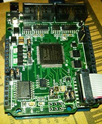
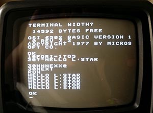 Maybe programmable logic isn’t your thing, and you’d just like a simple computer like the Ohio Scientific or the Apple I. The L-Star is for you. That’s [Jac Goudsmit]’s build featuring a 6502, a Parallax Propeller, and little else.
The Parallax Propeller is a powerful (multi-core!) chip that’s easily capable of handling video out, keyboard in, and serving up the ROM and RAM of a computer. [Jac]’s build does it all beautifully, and if you’re looking for the easiest way to run code on a 6502, this is how you do it.
6502s were found in just about everything, and while poking around at the local e-waste recycler, he stumbled upon something rather interesting. The case badges screamed, “BS medical device”, but after poking around a bit, he figured out this was an MTU-130 system, a machine that was apparently the top of the line in its day.
There’s some weird stuff going on in this machine – 18-bit addressing and 80kB of RAM. So far [Eric] has managed to dump the ROM, and he’s taking a look at the floppy controller board to see if he can figure out how it’s mapped. It’s one thing to figure out what’s broken on an Apple II or C64; those are well documented machines. It’s another thing entirely to figure out a machine very few people have heard of, and we tip our hat to [Eric] and his efforts.
 Here’s a build that both does and doesn’t have a 6502 in it. [BladeRunner]’s SheMachine is a single board computer that has a 65c816 in it. The ‘816 is an interesting beast that operates as a standard 6502 until a bit is flipped in one of its registers. After that, it has a 24-bit address space for addressing 16 Megabytes of memory, 16-bit registers, but is still completely backwards compatible with the 6502. Yes, it does have weird interleaved address pins, but we can only imagine what the world would be like if this chip came out a few years earlier…
[BladeRunner] is designing the SheMachine with 1MB of SRAM – more than enough, really – and is mapping all the memory through a CPLD. That’s how you should do it, anyway.


Here is a 6502 emulated on a chipKIT board:
http://wiki.kewl.org/dokuwiki/projects:ape65
I wonder if his new opcodes conflict with the 6510, which was the slightly-hacked-up version of the 6502 in the C64. (Commodore ended up owning MOS Technology, which was one of the reasons they could develop new machines faster than some of their competitors. One of the engineers there used to tell the story of finding a bug in his chip design, making the fix and having the new silicon in hand in less than a week.)
Well, first off, he’s implementing something between a 65C02 and a 65816, so it’s already not exactly the same as an NMOS 6502.
Also, 6510 is the exact same ISA as the 6502. It just adds two memory-mapped registers for the on-die I/O port at $0000 and $0001.
Did the 6502 also allow the various undocumented ops that you get from filling in multiple bits in the various fields where the documented ops only had one bit filled in at a time? I only ever played with the 6510.
Yeah, they all had the same funny LAX/SAX/DCP/ISC/RLA/RRA/SLO/SRE instructions.
Let’s not forget about the most impressive 6502 project of them all, Bender Rodriquez!
http://spectrum.ieee.org/semiconductors/processors/25-microchips-that-shook-the-world
Didn’t the Super NES use a 65816? Or was it some variant?
Looks like a variant based on what wiki says:
The CPU is a Nintendo-custom 5A22 processor, based on a 16-bit 65c816 core. The CPU employs a variable bus speed depending on the memory region being accessed for each instruction cycle: the input clock is divided by 6, 8, or 12 to obtain the bus clock rate. Non-access cycles, most register accesses, and some general accesses use the divisor of 6. WRAM accesses and other general accesses use the divisor of 8. Only the controller port serial-access registers use the divisor of 12.[49]
http://en.wikipedia.org/wiki/Super_Nintendo_Entertainment_System#Central_processing_unit
I’ll just leave this here.
http://quinndunki.com/blondihacks/?page_id=1761
*wanders out, whistling softly*
I have some of those weird IDE/solid state disk things for you, btw…
Hey Quinn,
Just thought I’d say thanks for being so in-depth with your articles, you inspired me to build my own 6502 system too!
Accidently touched report comment while scrolling on my android phone.
I’m a newish developer in the toy industry and holy shit do alot of toys still use a 6502 based core…