You can etch a simple PCB at home with a few chemicals and some patience. However, once you get to multilayer boards, you’re going to want to pay someone to do the dirty work.
The folks behind the USB Armory project visited the factories that build their 6 layer PCB and assemble their final product. Then they posted a full walkthrough of the machines used in the manufacturing process.
The boards start out as layers of copper laminates. Each one is etched by applying a film, using a laser to print the design from a Gerber file, and etching away the unwanted copper in a solution. Then the copper and fibreglass prepreg sandwich is bonded together with epoxy and a big press.
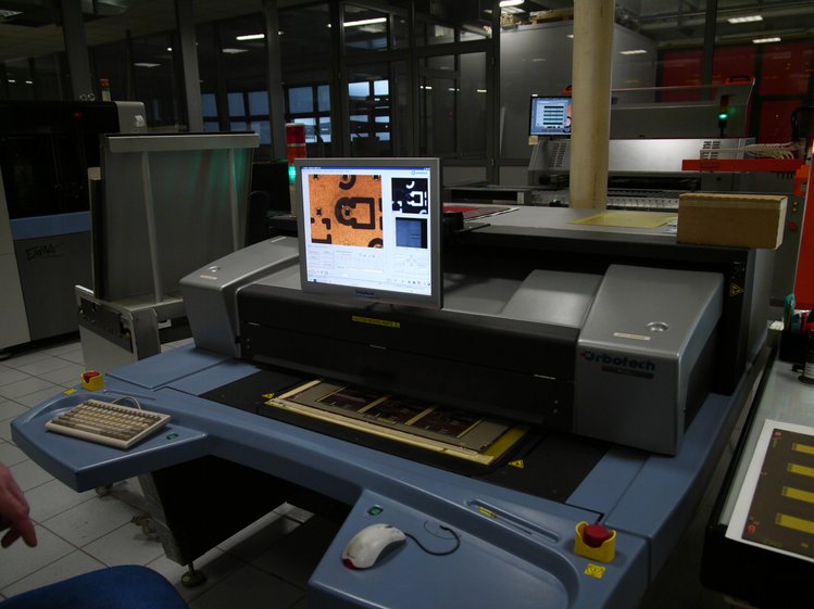
Bonded boards then get drilled for vias, run through plating and solder mask processes and finally plated using an Electroless Nickel Immersion Gold (ENIG) process to give them that shiny gold finish. These completed boards are shipped off to another company, where a pick and place followed by reflow soldering mounts all the components to the board. An X-Ray is used to verify that the BGA parts are soldered correctly.
The walkthrough gives a detailed explanation of the process. It shows us the machines that create products we rely on daily, but never get to see.


I call dibs!
Very impressive. Huge process in comparison to my double layer pcbs etched by myself :D.
Yeah, that’s an amazing process. We have some boards built that are 13 layers!
Eurocircuits has this nice video of their 4L PCB manufacturing process : http://www.youtube.com/watch?v=sIV0icM_Ujo
Came here to say exactly this.
Is any similar factory tour through the low cost $9.99 / 10 boards fabs ?
wait wait wait, did that guy in the video just say they use PALLADIUM to prime holes for plating???!
Next step – nanotech assemblers (ala Gibson).
If only you could do that cost-effectively within a chip package. In small runs.
It’s called an FPGA.
Try doing RF or analog on that ;)
It actually looks like the qfn have small gas pockets under the tab . Some manufacturers say that you should place vias in the tab which are untented on the opposing side so that the air can be drawn out..
Wouldn’t a plasma solution be better than chemical etching? This website explains the difference: http://www.plasmaetch.com/pcb-etching-machines.php