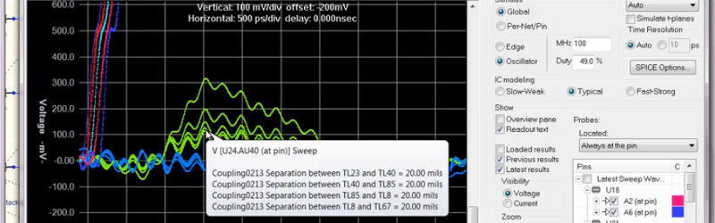
A link to this video demonstrating PCB cross-talk ended up in my mailbox the other day as I tend to stay on the mailing lists of the some of the high end CAD companies. There are some really interesting and powerful “mega-tools” that do things like plot noise density for decoupling analysis and extremely high speed timing analysis, though the costs of these tools are commensurate with their capabilities. This one is part of the Mentor Graphics PCB Simulation software.
The tool shown does the math needed to predict the induced voltage noise (cross-talk) generated by the proximity of noise sources to the noise susceptible elements, and the tool does so interactively. This is remarkable… in the past we would calculate some examples of trace width, spacing, and the type of signals involved, and then generate some rules of thumb that we tried to apply during the layout process. It was an educated guess that was sometimes not as close as we would have liked.
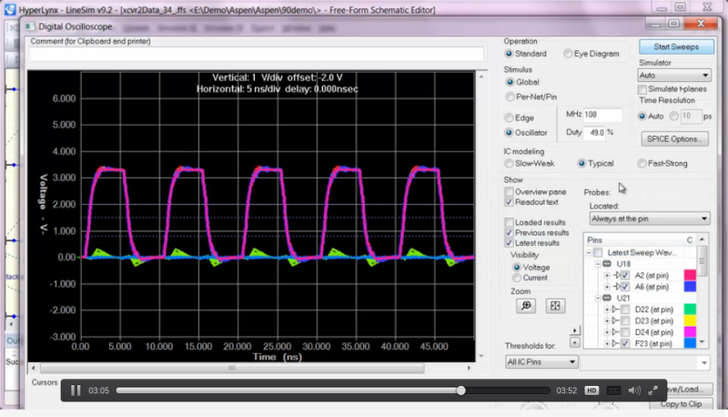
The cool part of this software is the interactive nature. One can learn the effects of placement on cross-talk in real time, which helps build an intuitive understanding.
I will add the standard disclaimer that a tool is exactly that, a tool, and it only represents an approximation of real life at best. It’s tempting to design to the tool itself, and many engineers have learned the limitation of a tool the hard way. Instead think of the tool as another opinion, or as mentioned, a learning aid to gather an intuitive feel for the effects of placement on circuit performance.


I’d kiss whoever could code software giving warnings on as many EMSEC/noise issues w/ a circuit as possible before they present themselves and screw w/ my head; that’d be an accomplishment for sure. I mean, think how much quicker it would make things (if it was good, like PSPICE++). Downside would be “locking into” pre-set designs and becoming reliant on it, meh…
These tools still require a very high level on understanding on SI background as the user is still responsible for feed it the right parameters – I/O models, bus topology etc. and is responsible for interpreting the results and correcting S/I issues.
There is no Star Trek simulation nor magical tools that replace the experience needed for a long while. These tool however improves on the accuracy by extracting the PCB trace parameters from a layout with (hopefully) a 3D field solver. (vs a crude 2D model by hand).
Jeez, it’s not a 3D field solver. We’re not talking about a $10k simulation package here. It’s a 2D field solver for cross-coupling.
Did JTAG ever approve analogue extensions? With little more than a comparator jaw droppingly amazing things open up.