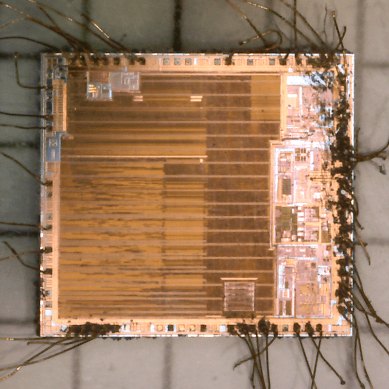
[Jelmer] got curious about the TI CC26XX wireless MCUs and did a little decapping.
TI sells four different models of their CC26XX wireless MCUs. Three support one of the following: RF4CE, Zigbee/6LoWPAN, and Bluetooth and a further model which supports all protocols. Each IC has the same baseline specification: 128Kb Flash, 20Kb RAM and 15 GPIOs.  [Jelmer] was curious to know if the price difference was all in the software. And in order to verify this decided that decapping was the only thing to do!
We’ve covered decapping using Nitric acid before, as well as lower tech techniques. Luckily [Jelmer] had access to Nitric acid and a fume hood, not the easiest items to get hold of outside of a research lab (checkout the video of the IC bubbling away below). [Jelmer] got some great die shots under an optical microscope and was able to confirm that the die markings are identical. This opens the door to future hacks, which might allow the cheaper models to be re-flashed, expanding their capabilities.


So buy the cheapest and when/if someone hacks the software, enable any or all the other features. Then watch as TI makes physical alterations to the chips to disable the functions.
Or they may already be binning them and programming according to which functions are defective on the die, so hacking to enable functions may not work or may not work *correctly*.
TI probably doesnt care if a few hackers start re-flashing their devices. The big money comes from big industry consumers, and those guys are unlikely to use a chip with hacked firmware in a production device.
On another note, I am willing to bet the different features are enabled/disabled through fuse bits, not standard flash, so it may be more difficult to unlock these features than people think.
Right, I don’t understand the assertions of crippleware without knowing the testing regimen that the ICs undergo. It’s quite likely that the more capable chip is tested to comply with some of the key RF performance specifications demanded by BLE, and testing costs money. Also, stacks don’t come free, so by including the BLE stack on the CC2650 TI is incurring a real cost with the stack vendor. Seems logical that the chip with that feature would cost more. On the flip side, from a design, verification, and production standpoint, it’s far, FAR easier to produce one die instead of two. Even if the 2630’s cost is burdened in some way by the extra functionality needed to meet the more stringent specs of the 2650, that cost is certainly recouped, probably manyfold, by binning and ancillary savings from not developing two die.
And why non of them comes with more than 1 UART ?! We are using the CC2541 and we wanted to move to the CC26XX series the second we heard the announcement. But our device has GSM and GPS on board so now we are stuck with the 8051 based CC2541.
You may still be able to use one of the CC26xx series parts. Typically the baud rates on GPS communications are low enough you can implement a UART in software using edge triggered interrupts and a timer.
Thanks for the suggestion.. I don’t have a great proof why, but I am really against software UART..
The integrated sensor controller on the chip can be set up as a second UART. Alternatively, if you do not need to use the UARTs at the same time, you can remap the UART to different pins when required.
The integrated sensor controller on the chip can be set up as a second UART.
That is interesting, going to look for more details now. Thanks
Nothing in this project tells me that this is crippleware.
It may just be yield optimisation.
Tuning parameters that are not precisely controlled in die manufacture may result in some chips having sub standard performance for a given protocol (frequency) rather than throw it away it could be sold for a protocol that it does come up to standard for.
This is nothing new to manufacture. Manufacturers will often use bits to disable ‘half’ of something like SRAM so that if there is a defect then the half which has the defect is disabled and the chip is sold and a lower featured version.
Reminds me a bit of those old 3 core AMD processors that were QC failed 4 core models with the defective core disables.
or the old Pentuim / Celeron series.
All the chip vendors still do this, and it’s not just frequency and core binning. Every block in modern SoCs has an associated yield risk and cost to fully test in production, so vendors stick in fuse bits to disable these features and logic to work around their absence. Caches, coprocessors, embedded GPUs, and just about everything else can be fused off in production. Sometimes they do this depending on market demand to “protect other product lines” by not offering the kitchen-sink feature set on entry level chips even if the die is the same.
This one is close to my heart. I’ve got an AMD-based MythTV system that would randomly froze and locked up solid for no reason that I could see (i.e., nothing in the logs). After many diagnostic attempts, replacing RAMs, tuning various kernel parameters, etc., I noticed that the system would run solid as a uniprocessor. Then I gradually increased it to dual, tri, and quad and found it only became unstable when it ran as a quad. A few months later I saw an AMD product announcement for a tri-core CPU line. Hm…
The price difference isn’t enormous and TI are (reasonably) happy to give away samples. Not something that is asking to be hacked IMHO – even if it is possible.
There are licenses related to some of the protocols. So they are most likely blowing some fuses while manufacturing to disable a given protocol and avoid playing the license fee for e.g. zigbee if it’s not needed by the customer.
It also improves yield and testing time as previously mentioned.
That’s standard procedure.. Btw. I used to work for Texas Instruments…
Nitric acid turns your fingertips yellow. You don’t realize it’s burning through your finger until it starts itching. (Also eats through rubber gloves eventually, which is how I came to learn about the first two!)
The four SKUs may be patent related — shipping the chip with only one protocol enabled means TI only has to pay patent fees to one licensee/pool. Typically chips like this come with royalties already paid so the end-user of the chip has no liability.
All companies do that. And they are smart to make sure simple patch can’t disable it. I worked for a semicon gain in mobile chips. We use to do only a single chip which comes to market as atleast 5-6 different SKUs with different features hit the market, controlled by fuses NOT by SW.