One day [Andy] was cruising around eBay and spotted something interesting. Forty Virtex-E FPGAs for two quid each. These are the big boys of the FPGA world, with 512 user IO pins, almost 200,000 logic gates, packed into a 676-ball BGA package. These are not chips designed for the hobbyist. These chips are not designed for boards with less than six layers. These chips aren’t even designed for boards with 6/6mil tolerances from the usual suspects in China. By any account, a 676-ball package is not like a big keep out sign for hobbyists. You don’t turn down a £2 class in advanced PCB design, though, leading to one of the most impressive ‘I just bought some crap on eBay’ projects we’ve seen.
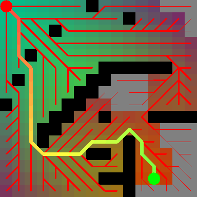
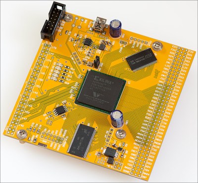 The project [Andy] had in mind for these chips was a generic dev board, which meant breaking out the IO pins and connecting some SRAM, SDRAM, and Flash memory. The first issue with this project is escape routing all the balls. Xilinx published a handy application note that recommends specific design parameters for the traces of copper under the chip. Unfortunately, this was a six-layer board, and the design rules in the application note were for 5/5mil traces. [Andy]’s board house can’t do six-layer boards, and their design rules are for 6/6mil traces. To solve this problem, [Andy] just didn’t route the inner balls, and hoped the 5mil traces would work out.
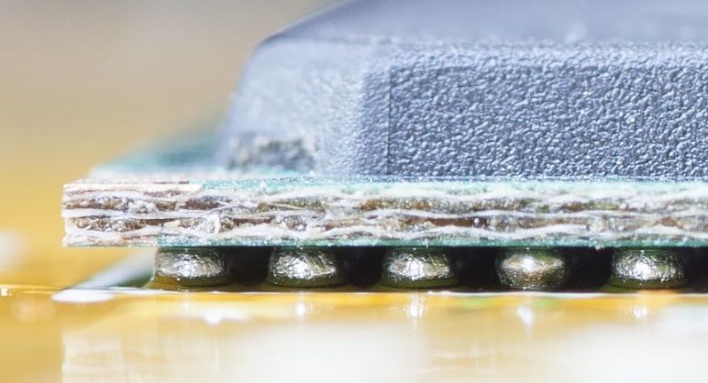
With 676 tiny little pads on a PCB, the clocks routed, power supply implemented, too many decoupling caps on the back, differential pairs, static RAM, a few LEDs placed just for fun, [Andy] had to solder this thing up. Since the FPGA was oddly one of the less expensive items on the BOM, he soldered that first, just to see if it would work. It did, which meant it was time to place the RAM, Flash, and dozens of decoupling caps. Everything went relatively smoothly – the only problem was the tiny 0402 decoupling caps on the back of the board. This was, by far, the hardest part of the board to solder. [Andy] only managed to get most of the decoupling caps on with a hot air gun. That was good enough to bring the board up, but he’ll have to figure some other way of soldering those caps for the other 30 or so boards.


Should get himself at least a cheap Mylar/Kapton solder stencil and at least a toaster oven to do reflow. A vacuum pipette is also handy, this can be built with a syringe, a needle (cut short) and any small “aquarium pump” like suction pump.
Given he says he’s got a reflow oven, I think a toaster might be a step backwards…
It’s a two sided board, so reflowing the capacitors on the back of the board would be difficult.
two sided reflow is standard procedure, you do one side at a time
[Andy] has a lot of balls.
I see what you did there.
He is also decidedly not a hobbyist. Check out his other board designs.
I think I’ve seen this chip before used on old mobile phone base stations.
Could be yes. Lucent equipment used them long back.
“These are the big boys of the FPGA world”
15K LUTs? Clearly you have some learning and perspective to develop.
Big boys of 70’s yes (not that old but it’s for the style) :D
Those old chip don’t worth a lot, unless your only goal is to learn
how to layout and assemble complex PCB…
70s? :) Maybe you need some perspective as well…
At my age late 90’s, early 00’s are far away :D
512 I/Os. That’s still big-boy nowadays. Logic isn’t everything.
For many projects, the number of I/Os is more of a downside than an upside. I don’t think he’s even managed to break most of them out. 15K LUTs is towards the mid-range of Altera’s low-end MAX 10 FPGA series, which they seem to be positioning as a replacement for CPLDs and which are available as single-supply devices with a QFP packaging option – much nicer to work with, at least in theory.
Kindof. I mean, if you don’t need the I/Os, don’t use the 676-ball package. Of course at some point you hit the smallest package in the family, and yeah, FPGAs tend to be bigger than they have to be, with the exception of the Lattice iCE40s, for the most part.
If you’re talking about this project in specific, though, then you have to consider the price tag. You’re not getting *anything* close to that chip’s performance and I/O count at $3-4/part.
That’s a fairly impressive job! Unfortunately the software needed to program that Virtex is likely a heck lot more expensive than the chips. I don’t think this Virtex is supported by ISE Webpack or the free version of Vivado or is it?
Don’t think it is freely available. Article explicitly states “latest ISE version to work with these chips is 10.1”, which kind of implies it’s not available as a webpack version. However, chances are you can get an old, no-longer-used license for that piece of software that no-one in their right mind would enjoy using
You’ll need one of the old archives releases, I believe the webpack versions of ISE8-9-10 supported VirtexE up 600 for free
“His” board house can’t do 6-layers and 5mil trace/space? So, why not just go to someone who can do it then?
I dont get why people artificially try to make stuff harder than it should be. 4-layers are cheaper you say? Well, if someone has enough money to impulse-buy a stack of FPGAs “just for fun” and make a pcb for them “just for fun”, the money argument seems extremely insignificant. The 6-layer board would not only help to get a good fan-out, at the same time you can make an extremely good decoupling cap with two internal planes and minimal prepreg thickness inside your pcb. I’m shure this would help a lot with stability, especially once you start to actually use a big chunk of that chips performance.
Something else that seems a bit strange to me, why would you do length tuning on a diff pair line, and at the same time, not do any length tuning on the parallel RAM bus? The SRAM is probably not that critical, but the SDRAM shure would love to have your clock, adress and data arrive in sync. Ok, shure, if you want to push the limits of these LVDS data ports, length tuning on top of diff-pair routing and general impedance control is nice, but then you would actually use a connector designed for high speed diff-pair transmission with defined signal impedances, and definately not connect it to a 0.1″ standard IO-header…
SDRAM is for 166MHz, so we are talking about 6ns period. Average propagation delay for microstrip is about 6 inches every ns. I would be surprise if those track skew are more than 0.5″ which means 100ps or 2% of the timing budget. That’s not worth fuzzing about.
Read title as “dying huge bga packages” and expected metallurgical gore.
Me too and expected side effects from tin whiskers, unreliable lead-free solder joints and similar modern plagues.
Am I the only one soldering 0402’s with a regular soldering iron?
Well, no. Except if it comes to desoldering where I use two regular ones. ;)
For desoldering 0402 I just take a lpt of solder on the tip and heat the whole component with it- it goes off nearly instantly.
Definately not. I go down to 01005 sizes with hand soldering.
Haven’t had the pleasure to do a design that needed smaller passives (008004 anyone?). Our assembly and reflow lines would have to get some serious upgrades to be able to pick and place and see these tiny components, and we do not see a good enough reason to upgrade our machines right now.
Check out mechatronic-systems.com very cheap, very capable.
Not a hack! This guy’s efforts are huge and totally professional, it seems that he just happens to do it in his spare time.
I’m not knocking the article, it is valuable information and fascinating to see how the professionals do things, much appreciated.