What does it take to go from concept to dropping a finished product into the hands of the end user? Gather ’round for a story that pulls people and parts from around the world to make one killer piece of hardware art.
Hosting a conference about hardware creation presents an excellent opportunity to build a hardware badge. But the bar is set pretty high — everyone looking at it will notice all the telltale signs of design choice, component selection, and manufacturing process. Luckily we had a great team working on the Hackaday SuperConference Badge and it turned out magnificently. Let’s look at what it took to get there.
Concept, Design, and Prototype
We already had a proven user interface from the Hackaday Belgrade conference. It was so interactive, and adopted with such joy, that it made a great starting platform for the SuperConference. All of the good was kept from that first iteration, but many changes were made to build the pleasing aesthetic that we arrived at.
[Voja Antonic] is the badge designer. He developed a striking badge shape, and laid out a visually fascinating LED matrix with the parts at a 45 degree orientation to the sides of the board. The battery holders were mounted straddling the edges of the board, and the matte black silk screen, button colors, and silk screen color all worked with each other. No, this product doesn’t have an injection molded case or other enclosure — some might think it an incomplete story of manufacturing without one. But the beauty of the hardware design would be lost if covered up.
After sending out the initial prototypes back in June, we had a winner and it was time to move toward manufacturing. If you find yourself longing for more details on the badge design check out [Voja’s] article on the topic.
Gathering the Materials and Finding a CM
[Chris Gammell] jumped in to drive the production effort. His first task was to review the Bill of Materials from [Voja] and this raised some question marks. [Voja] lives in Belgrade, Serbia and had selected parts that were only available from one supplier: Comet Electronics in Belgrade. This includes a few difficult to replace items (at least without changing the design) like the buttons and the constant current LED driver.
The decision was made early to minimize the number of single-supplier parts, carefully check stock, and make sure we had the parts in hand in time for manufacturing. The majority of the components are stocked by numerous distributors — stock counts and price were carefully considered when choosing Digikey for the rest of the order.
Assembling 300 boards is an interesting challenge. Contract manufacturers handle orders of 300 boards all the time, but normally they are not as complex as this badge. [Chris] reached out to multiple CMs for quotes and narrowed down the field. We ended up going with our friend [Bob Coggeshall] who is the founder of Small Batch Assembly in the Washington DC area. [Bob] is a friend of Hackaday — we interviewed him about his role in inventing the unix ‘sudo’ command a couple of years ago and have run into him several times since. It’s nice working with people you know.
Assembling the Boards
 [Bob Coggeshall] jumped right in, working to get the design ready for the smoothest possible production techniques.
His first step is to review the solder paste Gerber files. These tell him which areas of the board have tight tolerances and may prove difficult. In our case there are two: the accelerometer and the USB connector. The accelerometer is an LGA-16 footprint with 0.5mm pitch (Small Batch Assembly’s limit is 0.45mm) and the USB connector is a through-hole part which will require intervention by hand for every part. After discussing concerns with [Chris] and [Voja], we decided to move ahead with the process.
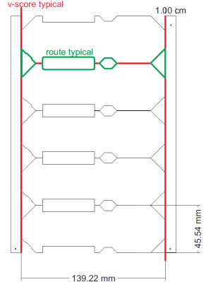
Next up is panelizing the PCB files. [Bob] bases this on the limit of his equipment — his reflow oven decides the max panel size. Next he sent the panelized file off to his friend [Rocky] at MG Circuit to ensure his plan of through-routed and v-scored panels was understood. This is a clever way to do things, since it allows boards with interesting outlines to be designed but the 4-edges with v-score still hold the panel together while being simple to separate after population.
The boards arrived looking fantastic, and during the wait [Bob] had already programmed his pick and place for the task — a process that took an entire day. His first order was to assemble one single panel. This was shipped to [Voja] for testing. Good news everyone, the panel performed magnificently. Time to head for full production!

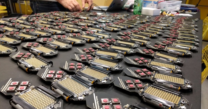
That complexity mentioned earlier? Every board had to have solder applied with a stencil, parts placed by machine, a trip through the reflow oven, and inspection… twice, since it needs to happen for both sides of the board. The back side was populated first, the front side, with 128 LEDs and various other parts came second. That front side took four minutes per badge (twenty minutes per panel) to pick and place. Complexity comes in the form of 50,000 parts placed on the 300 boards, an assembly time of about 30 hours all-in.
Testing, Rework, and Final Assembly
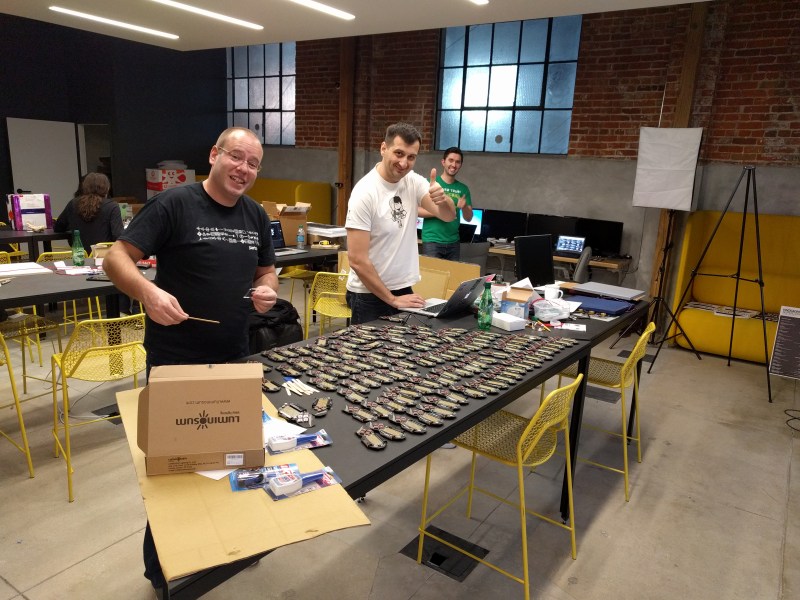
Assembled badges were shipped to the Supplyframe Design Lab in Pasadena about two weeks before the SuperConference. These came as five-to-a-panel units and required several steps of final assembly.
First, boards needed to be depanelized … a simple matter of applying some force to the v-scored areas. Because they had been on panels, the edge-mounted battery holders weren’t yet populated. [Voja] set to work hand-soldering 600 of the AAA battery holders (two per boards).
Next came flashing the firmware and testing every single board. Failure rate was about 7.5%, with the accelerometer being the culprit most of the time. This was one of the two ‘trouble’ parts [Bob] raised at the start — the fine pitch makes solder paste alignment critical and the package has no visible leads so visual inspection is impossible (you’d need to use X-ray). [Chris Gammell] reworked these by lifting the chip with hot air, hitting it with a flux pen, and reapplying again with hot air. This got almost every defect board working.
Continuing with mechanical assembly, we added the acrylic bezel which adds rigidity to the battery holders, and looks great. The Design Lab has a laser cutter so fabbing these bezels was the easy part. The problem is that laser-cut acrylic has a coating which needs to be removed from both sides and these parts are super narrow making it hard to peel. [Marco] spent most of a day removing the film and working with [Dusan] to super-glue them in place. The next wrench in the works was the lanyard clips which were too large for the hole in the PCB. The solution was to use pliers to open the eyelet, removing the clip and inserting the badge before closing it again.
The final step was to reflash each badge with a unique serial number which would serve as the gate-keeper for the IR communications.
Hardware is Hard
It’s pretty amazing that this came together, and the tale of manufacturing wouldn’t be complete without looking at some of the ways we tilted the scale in our favor.
We set out with a BOM cost goal of $20 including assembly. There are many ways to bend the numbers but a reasonable fence-sitting estimate is that we overshot that by around 20%. But that number doesn’t include some of the costs which we didn’t have to directly pay: the cost of the hardware design, a project manager, and final assembly and testing are not included. Also, Small Batch Assembly gave us the “Friends of Hackaday” rate which we were very happy to get. And our friends at Microchip, Garrett Scott specifically, threw in their time and talent to upgrade our bootloader to work as a USB mass storage device.
These extra costs that aren’t included in the bottom line but they all tied in to make this project magic. Most conferences don’t have the latitude to take on something this risky, but Supplyframe made these badges a priority and that let use roll the dice and make it happen.
Anyone who attended the SuperCon will agree, this was all worth it. The badge we have is a beautiful piece of electronics that shows our love for the design, the process, and the culture that go into hardware creation. It’s the perfect embodiment of what Hackaday is all about, and sharing the process here is a continuation of that spirit.


Great article!
This deserves to be redone as a longer article with more detail from the people involved. For a product beta test run it’s about the right size. I’m sure there are a lot of “minor” details not covered that are quite important for someone trying to launch a consumer product. There have been several other good articles about small run manufacturing. Could they be combined into a book on small run electronics manufacturing with lists of vendors? It would be even better if there were a section on packaging, marketing and sales. There has been good coverage of all these on HaD, but it’s spread out and not easy for someone to find all the relevant articles.
FWIW Here are some videos of the first badge being stuffed by the pick and place; The machine halts because the film isn’t coming off of one of the reels of parts; A very common occurrence on initial startup. https://www.youtube.com/playlist?list=PL7LPp3wY45hvc-doo_1w10G9Ksw-Ezeef
Question: it looks a bit slow compared to other machines I’ve seen. Is this done at lower speed? And if so, why?
my guess is that it’s the debug speed.
The speed in the video is the speed of the machine, an Manncorp MC400. Roughly 5k placements per hour. You are probably looking at machines like the 25k placement per hour Samsung like Adafruit has or the 120k placement per hour Mycronic like Sparkfun has. Those machines also cost 4 to 6x what the MC400 does.
That LED P&P reminds me of LED fixture manufacturing.
So, what did the cost per board end up being? Also, what was the total cost?
Actually, Marko and Dusan soldered 600 battery holders, not me. I was so unlucky to pick some terrible virus at the worst possible moment, so I was very ill that day and I spent the whole day praying for death in my room in Pasadena :D
That was a very nice read.
Thank you for that contribution.
I am in charge of production myself and over the years I had some very frustrating and very englightening experiences with hardware manufacture.
The key lessons learned are:
– China is NOT much cheaper than your local companies unless you make thousands of something
– ALWAYS make prototype runs till the design is 100% perfect. Never change anything on a prototype and have PCBs manufactured in a large scale. Just don’t.
– If the offer from your CM seems to be too good to be true, it is probably not true.
– Always calculate 10% defective boards that need rework. Usually it’s less but when you deal with large numbers leave enough space for unexpected failures.
Maybe I will make a little writeup on the MagicShifter Development.
I learned a lot during these days..
amen !
Great to learn more about the behind-the-scenes work. Kudos to Chris for some keen rework, those accelerometers are teeny!
How do they program the p’n’p machine? I was quoted 500€ for programming for a batch, here you write “one day” (which is consistent with the price I got). From the outside, I give them the components placement and orientation, it feels like they just have to do the reel position and correct for panelization, where is the time spent? I would really like to see a video of someone explaining their job.
The simple answer is “it depends” There isn’t the same level of standardization on PNP machines as there is on PCB manufacturing. Most contract houses end up creating custom scripts and processes to convert from the various board design tools. The basic Centroid file used is essentially just a list of X/Y coordinates. The CM has to load feeders and tell the machine the orientation of the part on the tape (so the machine rotates the part the correct number of degrees). There are also some hassles related to the machine’s placement accuracy that may require additional fiducials and the like. Plus many houses will have several machines tied together into a line, and someone has to manually decide which machine will place which parts. (They might have a chip shooter to place a large number of identical parts quickly like decoupling caps, or the LEDs in the badge. A different machine might be equipped with better accuracy, or a upward camera allowing it to place fine parts with a greater accuracy, etc) The scary thing is a lot of manufacturers can’t or don’t want to bother importing a file.. they do the programming with a teaching pendant for each job.
I program our pick and place at work from time to time. Ideally we would have a technician in charge of that, but in reality all of ours seem to have too little patience with software / computers to get through it. In an ideal scenario, yes, it would be simple. Load the reels of parts, stencil, and drop in your table of components/coordinates and you’re set.
In the real world, generally the vision system has standard packages which don’t exactly match your parts manufactured dimensions/pitch. This has to then be corrected by teaching the vision system the correct package shape/centroid, or manually programming the package by hand. Also, don’t expect the package to match the datasheet. Just because the BOM may have the x/y coordinates of the parts, that doesn’t guarantee the footprint was laid out around the centroid of the part. Some modifications might have to be made. I generally end up importing it to a spreadsheet to make these corrections. Also, expect everyone to have a different convention for laying out diodes, polarized caps, etc. Those generally require some correction too.
Some components require special settings. For instance, large electrolytic caps or ICs can’t handle the acceleration /deceleration that an 0402 can. That means, for that package, settings may have to be modified so that the part doesn’t get dropped.
Those issues take up the bulk of the time. Others may have to do with solder paste viscosity or stencil issues. Smaller solder pads become problematic when there’s more surface area around the perimeter of the pad (the etched wall of the stencil) than there is area of the pad itself. In this case you run into issues with solder paste getting lifted by the stencil and have to tweak application pressure settings, etc. to get the board properly pasted.
Lastly, there tend to be some issues with the reels. Smaller runs are more difficult because you may have cut tape and have to splice a lot of the tape and backing. I think the tape has problems breaking or not peeling on just about any machine.
As you can see, there are plenty of things that can go wrong. That said, I’ve had a couple jobs that went very smoothly and were running within a few hours, but that’s not the norm. Typically I allocate a day, or maybe two for more complicated boards just to get the first panel off the line. After that, it’s a piece of cake – mostly just fixing feeder problems every now and then.
We run an essemtec line. Pretty slick machines. The PnP does 16K parts/hr with four heads and an automatic tool changer. That said, the software is a bit counter-intuitive at times. We generally just chalk it up to being Swiss. Also, you don’t want to disable the safety lockout on it as it can move its arm much faster than you can get yours out of the way. All in all, pretty mesmerizing to watch. I think, to get much faster than our machine, the designers would have to pay special attention to the kinematics. There are already a lot of vibrations introduced by the incredible speed of the machine (it’s moving belt driven h-bridge style gantry/tool-head) which are tolerated for the most part due to the mass of the machine.
Pretty much the tasks are: Review of CAD, Receiving, inspecting and inventorying parts and boards, Verifying, possibly editing, then ordering or cutting the stencil(s), Paste and Stencil jig setup, Then basic PnP machine setup for the PCB. After that, for each BOM line item the part must then be mounted on the feeder, correctly associated with the PCB’s XYR placement list, then machine vision programmed and a test pick performed. For jelly-bean resistors and capacitors the machine vision has a library which shortens the process, but most ICs the machine vision has to be taught “from scratch” which can add a few minutes. So yes, anywhere from a good chunk of the day to all day.
Here are some more vids of the MC400 feeder mounting process. https://www.youtube.com/playlist?list=PL7LPp3wY45huVxFs-HOImcqsSSCMv0oK6