The Linux kernel recently added support for loading firmware into an FPGA via the FPGA Manager Framework. [OpenTechLab] has built a driver for the Lattice iCE40 FPGA (same chip used on the iCEStick and other development boards). One attraction to the iCE40 is there is an open source toolchain called iCEStorm.
Even if you aren’t specifically interested in FPGAs, the discussion about Linux device drivers is good background. The principles would apply to other drivers, and would definitely apply if you want to write another FPGA loader.
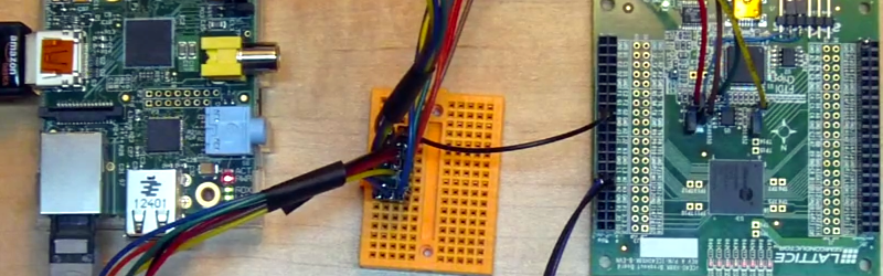
The example uses a Raspberry Pi connected to an evaluation board. A cheap Sigrok-based logic analyzer let him troubleshoot and debug. If you think FPGA development is expensive, think again. The board used here is well under $50 and the software is free. An iCEStick is even cheaper, and would probably work here, too. You are likely to have the other bits, but even if you need to buy a Pi and the logic analyzer, the whole thing is way under $100.
We’ve covered the iCEStick and iCEStorm quite a bit in the past. There are also quite a few iCE40 boards for the Raspberry Pi that ought to work well with this, including this one.


Given there are some rather creative iCE40-based FPGA boards coming out (e.g. Olimex did one late last year based on the iCE40-HX1k with some nice add-on peripherals) this raises some interesting prospects for interfacing these chips.
I hope with time Lattice consider something in a more accessible form factor than QFN32 or TQFP80, not all of us have the facilities for making boards for and soldering such tiny packages.
But there are iCE40/iCE5 Ultra Plus and Ultra Light in QFN32\QFN48. I designed simple and cheap board with iCE5LP2K-SG48. Soon I will create a project with it.
Yep, tried a QFN32 chip recently… pain in the arse to solder, and the pitch is well and truly beyond what I can achieve without outsourcing.
A DIP can be slapped into a breadboard for experimentation and mounted to a circuit board in a variety of ways for production use.
SOIC and LQFP doesn’t fit in a breadboard but is still not too bad for home experimenting.
Anything else, and you more or less have to buy in adaptors or get a board made. Why use an adaptor board when packages exist that plug in natively?
The market for DIP40 packaging is so small for an IC such as this that you’ll never see a DIP40.
Be glad you’re getting QFN/TQFP – most FPGA companies are making 80%+ of their product in BGA configurations only.
That would be because you are doing it wrong most likely… QFN is one of the easiest fine pitches to solder all you have to do is align the pads, flux it to death and drag solder the pins which are much less likely to bridge due to thier not being parallel metallized areas for bridges to form.
Some chips only come in QFN … so enabling yourself to solder those opens up a lot of options.
If you wear glasses a cheap USB microscope would make it much easier too…. I can check alignment with a jewellers loupe for now… but I imagine the day will come I’ll need a scope.
QFN32 with a pin pitch of 0.5mm is pretty easy to solder if you’ve got a chisel tip of about 3mm or a hollow/well type tip about the same size. I’ve also soldered a tqfp64 PIC32MZ with a pin pitch of 0.4 which was a bit harder but still possible. The main problem was my laser printer transfer using an iron was a bit problematic to get the fine pitched pads to not smudge into a smear. I’ve reworked a 0.3mm pin pitch on a proper PCB with a solder mask without much trouble. Just a lot of flux and desoldering braid to remove bridges. Look on youtube for techniques with normal soldering irons, it’s a good skill to have. A hot plate or pre heater (or any plate that is temperature controlled like a 3D printer heated bed) is also very handy to have, makes it much easier to solder with lower iron temperatures.
What about IceZum Alhambra? (https://github.com/FPGAwars/icezum/wiki)
The market for modern programmable logic devices (e.g., FPGA/CPLDs) is being SERIOUSLY hampered by the Manufacturer’s ignorance of simplifying the tool chain for non-high quantity customers. The development environments, while crippled and “free” are BLOATED and impossible to use for new adopters at an individual level. There are some efforts to chop away at this (I think there’s a basic relatively open dev but tool-chain an programmer for these ICE parts that appeared recently, but the name escapes me). For example, the Xilinx CoolRunner CPLD line could become the “Arduino” of programmable logic devices, with all the free “future customers” that such an environment creates if ONLY Xilinx didn’t require a HUGE download, massive MSR, and ball-and-chain web-based real-time licensing just to be able to simulate then program the little device! Wake Up Altera/Intel and Xilinx!!
See https://github.com/FPGAwars/icestudio
@q2dg
Thanks for the reminder. IceStorm was/is the Reverse-Engineered effort I couldn’t remember at my original post time (more links about this below).
But – the IceStorm/icestudio “solution” is not what I was really aiming at, it was the FPGA/CPLD manufacturers that are suffering from BLOAT in their toolchains, even their relatively simple CPLD-like devices. Plus the likes of IceStorm & icestudio don’t have part-specific simulation (which realistically only the Manufacturer’s can provide), they fall back on the likes of Icarus Verilog. And the likes of IceStorm target only one family of parts.
* Some related links that are valid as of my post time:
– icestudio graphic editor for open FPGAs. Built on top of the IceStorm project
https://github.com/FPGAwars/icestudio
– IceStorm Project
http://www.clifford.at/icestorm/
https://hackaday.com/tag/icestorm/
– Platform lattice_ice40 <- this is the PlatformIO IceStorm bundle attempt
http://docs.platformio.org/en/latest/platforms/lattice_ice40.html
– Icarus Verilog Simulator
http://iverilog.icarus.com/
I love the iCE40 and the IceStorm flow. I used a Lattice HX8K development board to learn Verilog and make an address decoder for my 6502-based computer. With the FPGA I can decode a single address from the 64K range to an I/O device rather than the usual coarse ranges of addresses. Then I got carried away and implemented a UART, SPI master and CPU-controlled clock scaling too. So much fun.
Nice Projekt, but realy buggy, do not try to learn Verilog using icestrorm, it’s a very hard way ;)
I just tested to load the ICE40 firmware using user space code, sysfs gpio and spidev. Work without any issue. No need to use a kernel driver and device tree definition.
Interesting how you do it. Any console log would really help.
We just released the ice4pi raspberry pi hat – https://www.hackster.io/lightside-instruments/the-ice4pi-ice40-raspberry-pi-hat-b24c2f