The Internet is full of low-speed logic analyzer designs that use a CPU. There are also quite a few FPGA-based designs. Both have advantages and disadvantages. FPGAs are fast and can handle lots of data at once. But CPUs often have more memory and it is simpler to perform I/O back to, say, a host computer. [Mohammad] sidestepped the choice. He built a logic analyzer that resides partly on an FPGA and partly on an ARM processor.
In fact, his rationale was to replace built-in FPGA logic analyzers like Chipscope and SignalTap. These are made to coexist with your FPGA design, but [Mohammad] found they had limitations. They also eat up die space you might want for your own design, so by necessity, they probably don’t have much memory.
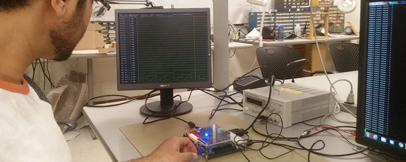
The system can capture and display 32-bit signals on a 640×480 VGA monitor in real-time. The system also has a USB mouse interface which is used to zoom and scroll the display. You can see a video of the thing in operation, below.
You can always opt for simulation, but sometimes you really need to run your design on actual silicon. There are subtle failures or even interactions with other hardware that are difficult to model in simulation.
There are several interesting design features to the analyzer, including the use of the Xillybus core to simplify interfacing from FPGA logic to the ARM AXI bus. This simplifies the communications with the ARM processor greatly.
We’ve looked at inexpensive FPGA-based logic analyzers before. You could use these integrated if you have any room left on your device. If you don’t feel the need for speed, you could opt for a CPU-based design.
If you couldn’t tell, this is one of the projects from [Bruce Land’s] students. Thanks [Bruce] for the tip and for what you do creating the next generation of hardware hackers.


Nice! The dev board used here (http://www.terasic.com.tw/cgi-bin/page/archive.pl?No=836) is the same one my Comp-E classes have been using, too. Seeing this is good motivation to learn to do the same stuff.
Nice work, but getting all the decoding done and allowing data transfer in a totally self contained unit seams a bit more trouble than it’s worth now that so many work benches have computers on them
I don’t get it. It would have been so much easier to have the capture utility dump to a file and then use any existing SUMP front end to view the data. Why re-invent the wheel? Once the data lands on HLS, you can do anything with it. Especially if it’s running Linux/X.
What’s a SUMP front end? Google doesn’t help.
http://lmgtfy.com/?q=sump+logic+analyzer
https://www.sump.org/projects/analyzer/client/
Also I was certain I had seen a similar project before. This guy:
http://www.frank-buss.de/parallella/sampler/index.html
He did it for analysis of external signals, however the same interface could be used for tapping internal signals in an on-board ZynQ design. And he did it in real-time which is a bit impressive….
your google-fu must be broken, https://www.sump.org/projects/analyzer/
I thought about that too. SUMP or even SigRok. However, as an educational exercise, I still think this was pretty cool.
An interesting solution but reading their write-up makes the premise feel slightly disingenuous; while it points out the limitations with Chipscope, etc and promotes the positives of their solution, without discussing the flip side – the limitations with their solution and where other synthesisable embedded debug capture blocks are more suited. It’s not that one solution is better than another (which their writeup seems to suggest) because they’re both targeting different problems.
As far as I can tell, this solution requires a (fast) processor core to be present in the FPGA logic, and for that processor to have spare (all?) processing time to host the debug capture/display side (which also means you’re potentially sharing the display output with functional items as well). What is nice is that it is fully managed (only need a screen and a mouse to run it) and an okay bandwidth whereas the embedded logic like Chipscope run on an external computer (plus JTAG dongle) but with a massive, short-term bandwidth.
At the end of the day it really comes down to how invasive/non-invasive debug you are happy with and where you can handle compromise – compare, on an ARM core say, the use of halting debug vs on-chip trace capture (ETM+ETB) vs external trace capture (ETM+Pins).
I believe this solution is targeted for Altera/Intel FPGA with HPS and Xilinx ZynQ series hybrid devices only. They both have an in-package ARM Cortex A series application processor complete with it’s own DDR3/4 memory controller. In both cases the fabric has a high-speed AMBA/AXI4 master tap on the SCU. This allows you to shove data into the ARM’s DDR memory directly and with automatic cache coherency. Think of it like a sigrok LA but instead of using an FX2 to push data to a capture host over USB, he is doing it more directly through the fabric.
Every FPGA coder has routed internal nets to external pins for connection to an off-board LA from time to time. But that technique can throw havoc into design timing. The main benefit tools like Chipscope offer is in synthesis. They give no route consideration to those intermediate taps. And if a net was previously optimized out, it stays optimized out and the effective intermediate tap is replicated in parallel logic.