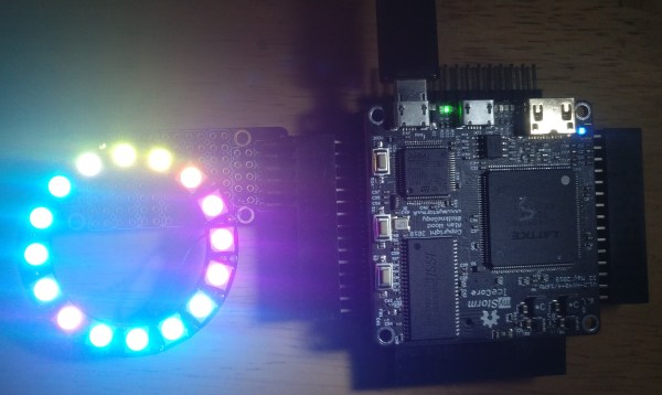
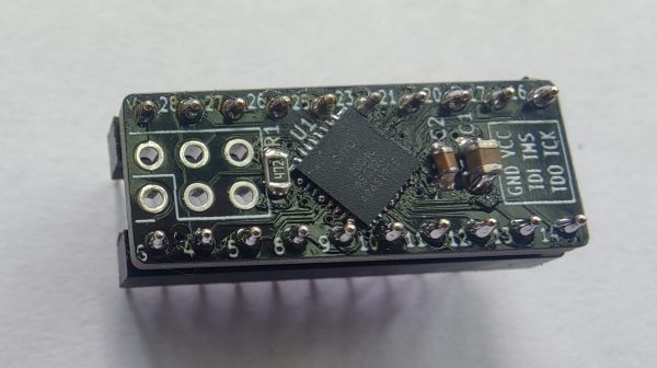
Stuffing an NES into an FPGA

megaman_fpga

When the developer of the µTorrent torrent client and the ScummVM  LucasArts adventure game interpreter gets bored, something cool is bound to happen. Luckily for us, [Ludde] was a bit listless over Christmas, and with more time than energy to burn, implemented a Nintendo Entertainment System on an FPGA dev board.

The NES was powered by a Ricoh 2A03 CPU, a chip nearly identical to the 6502 found in the Commodore 64s and Apple IIs of the early 1980s. There are a few differences between the two, though: the NES CPU includes an Audio Processing Unit on the chip and is connected to a very cool Picture Processing unit elsewhere on the NES. [Ludde] put all these chips in his Spartan-6 FPGA with a lot of Verilog code.

The rest of the system – the RAM, display output, and controller input comes from the peripherals attached to the FPGA dev board. [Ludde]‘s specific board didn’t have a good digital to analog converter, so the composite output was traded for a VGA output. It’s not a completely accurate color pallet, but it’s still an amazing piece of work for someone who was simply bored.

Ask Hackaday: We might have some FPGAs to hack

rear

[Chris] is an IT guy for a medical clinic up in Alaska, and until very recently the systems he monitored, fixed, and beat with a wrench included over 100 Pano Logic “Zero Client” thin clients. Pano Logic just went out of business and all support for these little boxes have been cut off, leaving [Chris] with a hundred or so very interesting pieces of hardware.

The idea behind these “zero clients” is the ideal of a thin client – take all the storage, processing, RAM, and other goodies and move them to a server. Pano Logic took this one step further than other thin clients, removing the CPU, memory, and basically everything you’d find in a thin client. What was left was a Spartan-6 FPGA, a few chips to drive the USB ports, a pair of HDMI chips, and a few DDR2 modules. Basically, [Chris] has about 150 FPGA dev boards just sitting in a storage room. The only thing that is needed is a bunch of software and an extreme amount of cleverness.

After opening one of these zero clients, [Chris] found a Spartan-6 FPGA right next to what he thinks is a 6-pin programming port. Along with the FPGA are a few other chips that would make any FPGA dev board a very neat tool:

We’re going to agree with [Chris] these Pano Logic zero clients show a lot of potential. If you’re up to the challenge of creating a very, very cheap FPGA dev board out of some discarded hardware, head on over to ebay or chat up your local IT guy.

Breadboard friendly FPGAs

fpga

Regular Hackaday readers will be familiar with all the cool things you can do with FPGAs; emulating old video game consoles, cracking encryption protocols, and DIY logic analyzers become relatively simple projects with even a modest FPGA dev board on your workbench. Many FPGA boards aren’t geared towards prototyping, though, and breadboard friendly devices are hard to come by. Here’s a pair of breadboardable FPGAs we’ve found while searching for some related hardware over the past few days

First up is the Mercury FPGA Module. Packaged in a DIP-64 format, the Mercury features a Spartan-3A FPGA with the equivalent of 200k logic gates. Elsewhere on the board is 512kB of RAM and 128kB of Flash storage. There are enough GPIO pins for nearly any project, but sadly only a 10-bit ADC – the same resolution you’d find in an AVR or PIC ‘micro.

Of course the Mercury isn’t the only breadboard-friendly FPGA dev board out there. There’s also the slightly more capable XuLA2 board powered by a Spartan-6 with 32 MB of RAM, 1MB of Flash. Unlike the Mercury, the XuLA2 can also fit in one of those ‘half-sized’ solderless breadboards.

Yes, it’s a different form factor than the commonly recommended Papilio One or the DE0. If you can suggest any other ‘beginners’ (i.e. doesn’t cost an arm and a leg) FPGA boards, leave a note in the comments and we’ll summarize them in another post.

Discrete FPGA will probably win the 7400 logic competition

For this year’s 7400 logic competition, [Nick] decided to build an FPGA out of logic chips.

Perhaps a short explanation is in order to fully appreciate [Nick]‘s work. The basic component of an FPGA is a slice, or cell, that performs boolean operations on its input and sends the result on its output. The core of these slices is a lookup table – basically a truth table that stores the result of every possible input combination.

One very easy way to implement a lookup table is to use a RAM or EEPROM chip. By tying the address lines of an EEPROM to the input and the data lines to the output, it’s possible to create a single slice of an FPGA very easily.

Unfortunately for [Nick], 74-series memories have long been out of production. There is another option open, though: shift registers. A shift register is basically an 8-bit memory chip with parallel inputs, so combining a shift register with an 8-input multiplexer is a very simple way to implement a 3-input, 1-output FPGA slice.

After figuring out how to tie these slices to bus lines, [Nick] needed a way to program them. Verilog or VHDL would border on insanity, so he wrote his own hardware description language. It’s certainly not as powerful or capable as the mainstream solutions to programming an FPGA, but it’s more than enough.

In the video after the break, you can see [Nick]‘s overview of his very large 8-slice FPGA while he runs a combination lock and PWM program. All the code, schematics, and board layout are up on [Nick]‘s git if you’d like to build your own.
[Read more...]

Storing user data on your FPGA

We’ve seen FPGAs used to recreate everything from classic arcade games to ancient computers, but with each of these builds a common problem arises. Once you’ve got the hardware emulated on an FPGA, you’ve also got to get the ROMs into the project as well. In a very interesting hack, [Mike] figured out that the serial Flash chip that stores the FPGA settings has a lot of space free, so why not store user data there?

[Mike] got the idea from seeing a recreation of the classic BombJack arcade game we featured last month. In that build, [Alex] needed to store 112Kb of game data stored in 16 ROM chips. Unfortunately, [Alex]‘s FPGA only had space for 40Kb of data. After realizing his FPGA had a 512Kb SRAM chip, [Alex] decided to put all the sprites, sounds, and levels of BombJack in the SRAM.

Impressed with [Alex]‘s build, [Mike] set to work generalizing the hack to work with other projects. [Mike] notes that only a few FPGA boards are capable of storing user data next to the  configuration bitstream; the hack is impossible on the Digilent Basys2 board, but it works wonderfully on a Papilio One 250K.

As a very cool build that makes FPGA-related builds even easier, we’ve got to tip our hat to [Mike] for writing up a great tutorial.

LVDS on an FPGA could make it possible to reuse laptops LCDs and the like

Search around the Internet and you’ll find a landfill of forum threads asking how to drive the LCD screen from a dead laptop. The answer is always that there is just no way to do it. That’s because most of them use a Low-Voltage Differential Signalling protocol that just isn’t available through the hardware used in hobby projects. But the appearance of this board could signal that things are about to change. We don’t want to get your hopes up too much. This isn’t an open source project, but it is a piece of hardware that can make LVDS available for the 8, 16, and 32-bit microcontrollers you’re used to working with.

It’s a derivative of a project [Thomas Jespersen] worked on for a customer. It uses an FPGA to implement the LVDS standard used by high-pixel-count LCD displays. It contains enough memory for a full frame-buffer, and includes a Motorola-8080 communication standard. [Thomas] gives a full description of how the setup works in the video after the break. Demonstrations start about 7:30 into the video with an STM32 F4 Discovery board driving the display.

[Read more...]

Homebrew FPGAs

Homebrew CPUs made out of logic chips are nothing new, but a homebrew FPGA is another matter entirely. [Joshua] sent in a project he whipped up where he made a single logic cell FPGA.

Despite how complicated and intimidating they are in practice, FPGAs are really very simple. They’re made of thousands of logic blocks capable of transmuting into AND, OR, NAND, and XOR logic gates. These logic blocks are all tied together, and with a somewhat complex hardware design language are capable of becoming a CPU, a micocontroller, or even a video card. Basically, programming a microcontroller tells a chip what to do, while programming an FPGA tells the chip what to be.

To build his single logic block FPGA, [Joshua] used a four-bit multiplexer to hard wire a truth table out of a 74HC174 D-type flip-flop. A bit of Arduino code changes the state of the pins connected to the multiplexer allows for any combination of TRUE and FALSE to be calculated for AND, NAND or XOR logic functions.

Yes, it’s only a single logic block for an FPGA, and if this build were expanded to even a few hundred cells it would be gargantuan. Still, there’s no better way to learn the ins and outs of abstract hardware, so we’ll gladly tip our hat to [Joshua] and his homebrew FPGA.