The $16 PCB Robot

It is a fun project to build a simple robot but, often, the hardest part these days is creating the mechanical base. [Concrete Dog] has a new open source design for stoRPer that uses a PC board as the base. The board has a Raspberry Pi Pico and motor drivers. The modular design allows you to add to it easily and use custom wheels. The video below shows some treaded wheels and some mechanum wheels with gears.

There are mounting holes for sensors and also a way to put another deck above to hold other circuits, power, or whatever you like. There’s lots you could do with this as a starting point.

Continue reading “The $16 PCB Robot”

Luggable Cyberdeck Can Still Be A Luggable PC

In the 80s and early 90s, there existed a class of personal computers that are no longer around today — the luggable. Planted firmly between a desktop and a laptop, these machines were lovingly called so because they were portable, but just barely. Think Kaypro, Osborne, or the Compaq Portable.

First things first — this lovely 1990-era industrial luggable has not been gutted according to [D1g1t4l_G33k]. The chassis, CRT, power supply, and ISA backplane are original and still intact, and they still have all the parts to restore it to its original DOS 3.1 form.

What [D1g1t4l_G33k] did do is replace the 386x-based ISA SBC with a 2005 AMD LX-600 Geode at 366 MHz. Gone are the ISA data acquisition cards and 80 MB SCSI hard drive, replaced with a 32 GB compact flash drive. The floppy drive is functional, too. Now it sits on a cart next to the workbench running AntiX Core 19.5, functioning happily as an AVR development workstation.

Having an old luggable to mess with in the first place isn’t a requirement. We’ve seen a modern take on the luggable, and here’s one with three monitors.

The FPC adapter shown soldered between the BGA chip and the phone's mainboard, with the phone shown to have successfully booted, displaying an unlock prompt on the screen

IPhone 6S NVMe Chip Tapped Using A Flexible PCB

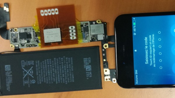
Psst! Hey kid! Want to reverse-engineer some iPhones? Well, did you know that modern iPhones use PCIe, and specifically, NVMe for their storage chips? And if so, have you ever wondered about sniffing those communications? Wonder no more, as this research team shows us how they tapped them with a flexible printed circuit (FPC) BGA interposer on an iPhone 6S, the first iPhone to use NVMe-based storage.

The research was done by [Mohamed Amine Khelif], [Jordane Lorandel], and [Olivier Romain], and it shows us all the nitty-gritty of getting at the NVMe chip — provided you’re comfortable with BGA soldering and perhaps got an X-ray machine handy to check for mistakes. As research progressed, they’ve successfully removed the memory chip dealing with underfill and BGA soldering nuances, and added an 1:1 interposer FR4 board for the first test, that proved to be successful. Then, they made an FPC interposer that also taps into the signal and data pins, soldered the flash chip on top of it, successfully booted the iPhone 6S, and scoped the data lines for us to see.

This is looking like the beginnings of a fun platform for iOS or iPhone hardware reverse-engineering, and we’re waiting for further results with bated breath! This team of researchers in particular is prolific, having already been poking at things like MITM attacks on I2C and PCIe, as well as IoT device and smartphone security research. We haven’t seen any Eagle CAD files for the interposers published, but thankfully, most of the know-how is about the soldering technique, and the paper describes plenty. Want to learn more about these chips? We’ve covered a different hacker taking a stab at reusing them before. Or perhaps, would you like to know NVMe in more depth? If so, we’ve got just the article for you.

We thank [FedX] for sharing this with us on the Hackaday Discord server!

Designing A USB-C Upgrade PCB For The MX Ergo Mouse

As the world of electronic gadgetry made the switch from micro USB to USB-C as the charging port of choice, many of us kept both of the required cables handy. But it’s fair to say that these days a micro USB port has become a pretty rare sight, and the once ubiquitous cable can be a bit elusive in the event that you encounter an older device that requires it.

[Solderking] has a high-end Logitech cordless mouse with just this problem, and so he replaced its micro USB socket with a USB-C port. That makes the task sound deceptively simple, because in fact he had to reverse engineer one of the device’s PCBs in its entirety, making a new board with the same outline and components, but sporting the new connector.

Instead of attempting to replicate the complex shape with geometry he started with a scan of the board and had Fusion 360 trace its outline before 3D printing a version of it to check fit in the Logitech case. Then it was a case of tracing the circuit, designing the replacement, and hand transferring the parts from board to board.

The result is a USB-C chargeable mouse, and while all the design files don’t appear to be online, it’s possible to download the Gerbers from a PCBWay page. On top of that there’s a YouTube video of the process which we’ve placed below the break.

This isn’t the first time we’ve seen somebody spin up a new board to add USB-C to an older device — this drop-in replacement for Sony’s DualShock 4 comes to mind. If you’ve got enough free space inside your particular gadget, you might be able to pull of a USB-C conversion with nothing more exotic than a hacked up Adafruit breakout board.

Continue reading “Designing A USB-C Upgrade PCB For The MX Ergo Mouse”

Replacement PCB Replicates Early 80s Modem

It’s certainly been a few decades, but plenty of us remember a time before widespread access to broadband internet, when connections were generally made over phone lines using acoustic modems. In the 90s these could connect you to AOL and Napster well enough, but in the early 80s the speeds were barely enough to read text as it loaded. A company called Hayes set out to change this with some of the first useful, widely-available modems for the PCs at the time. While they couldn’t keep up with the changing times there’s still a retro community that has these antiques, and to modernize it a bit this drop-in replacement for the PCBs replicates these old modems almost exactly.

The new PCB is equipped with everything needed to get a retro computer online again, including all the ports to connect a computer without any further modifications. It houses a few modern upgrades beyond its on-board processors, though. Rather than needing an actual acoustic coupled phone, this one has an ESP32 which gives it wireless capability. But the replacement PCB maintains the look and feel of the original hardware by replicating the red status LEDs at the front, fitting into the original Hayes cases with no modifications needed at all, and even includes a small speaker through which it can replicate the various tones, handshakes, and other audio cues that those of us nostalgic for this new online era remember quite well.

For those looking for a retro feel without the hassle of getting antique networking equipment functional again, this type of upgrade that preserves the essence of the original hardware is an excellent way of keeping retro computers functional on modern networking equipment. But if you absolutely must get the networking equipment exactly right down to the last patch cable, you might end up having to build your own ISP from scratch.

Continue reading “Replacement PCB Replicates Early 80s Modem”

Mapping The Nintendo Switch PCB

As electronics have advanced, they’ve not only gotten more powerful but smaller as well. This size is great for portability and speed but can make things like repair more inaccessible to those of us with only a simple soldering iron. Even simply figuring out what modern PCBs do is beyond most of our abilities due to the shrinking sizes. Thankfully, however, [μSoldering] has spent their career around state-of-the-art soldering equipment working on intricate PCBs with tiny surface-mount components and was just the person to document a complete netlist of the Nintendo Switch through meticulous testing, a special camera, and the use of a lot of very small wires.

The first part of reverse-engineering the Switch is to generate images of the PCBs. These images are taken at an astonishing 6,000 PPI and as a result are incredibly large files. But with that level of detail the process starts to come together. A special piece of software is used from there that allows point-and-click on the images to start to piece the puzzle together, and with an idea of where everything goes the build moves into the physical world.

[μSoldering] removes all of the parts on the PCBs with hot air and then meticulously wires them back up using a custom PCB that allows each connection to be wired up and checked one-by-one. With everything working the way it is meant to, a completed netlist documenting every single connection on the Switch hardware can finally be assembled.

The final documentation includes over two thousand photos and almost as many individual wires with over 30,000 solder joints. It’s an impressive body of work that [μSoldering] hopes will help others working with this hardware while at the same time keeping their specialized skills up-to-date. We also have fairly extensive documentation about some of the Switch’s on-board chips as well, further expanding our body of knowledge on how these gaming consoles work and how they’re put together.

PC AT mainboard with both 16-bit ISA and 32-bit PCI slots. (Credit: htomari, Flickr)

How Intel Gave Us The PCI Bus While Burying VESA’s VL-Bus

Gigabyte GA486IM mainboard from 1994 with ISA, VLB and PCI slots. (Credit: Rjluna2, Wikimedia)

The early days of home computing were quite a jungle of different standards and convoluted solutions to make one piece of hardware work on as many different platforms as possible. IBM’s PC was an unexpected shift here, as with its expansion card-based system (retroactively called the ISA bus) it inspired a new evolution in computers. Of course, by the early 1990s the ISA bus couldn’t keep up with hardware demands, and a successor was needed. Many expected this to be VESA’s VLB, but as [Ernie Smith] regales us in a recent article in Tedium, Intel came out of left field with its PCI standard after initially backing VLB.

IBM, of course, wanted to see its own proprietary MCA standard used, while VLB was an open standard. One big issue with VLB is that it isn’t a new bus as such, but rather an additional slot tacked onto the existing ISA bus, as it was then called. While the reasoning for PCI was sound, with it being a compact, 32-bit (also 64-bit) design with plug and play and more complex but also more powerful PCI controller, its announcement came right before VLB was supposed to be announced.

Although there was some worry that having both VLB and PCI in the market competing would be bad, ultimately few mainboards ended up supporting VLB, and VLB quietly vanished. Later on PCI was extended into the Accelerated Graphics Port (AGP) that enabled the GPU revolution of the late 90s and still coexists with its PCIe successor. We covered making your own ISA and PCI cards a while ago, which shows that although PCI is more complex than ISA, it’s still well within the reach of today’s hobbyist, unlike PCIe which ramps up the hardware requirements.

Top image: PC AT mainboard with both 16-bit ISA and 32-bit PCI slots. (Credit: htomari, Flickr)