Capacitive Touch Controller For FPGAs

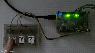
Most projects that interface with the real world need some sort of input device. Obviously this article is being written from a standardized “human interface device” but when the computers become smaller the problem can get more complicated. We can’t hook up a USB keyboard to every microcontroller since we often only need a few buttons, but even buttons can be a little bit too cumbersome for some applications. For something even simpler, we would like to turn your attention to capacitive touch controllers.

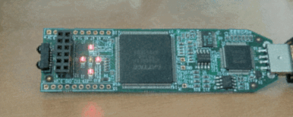
Granted, these devices are really only simpler from a hardware perspective. Rather than a switch that can be prone to failure either when its moving parts break or its contacts become corroded, a capacitive touch button only needs a certain conductive area on something like a PCB, along with a few passive components, to work. The real difficulty is in the software, so this project aims to make it simpler to bring these sort of devices to any FPGA that needs some sort of interface like this. It can operate in stand-alone mode or in a custom user interface, and was written to be platform-independent in VHDL without the need for any dependencies or macros.

The project’s page goes into a great amount of detail on how capacitive touch sensors like these work in general, and describes the operation of this specific code as well. Everything is open source, so it’s ready to be put to work right away. If you need capacitive touch capabilities on something like a microcontroller, though, take a look at this tiny Atmel-powered musical instrument instead.

A Game Boy connected to a monitor while playing Super Mario Land 2

FPGA Boards Add VGA And HDMI Interfaces To The Original Game Boy

The classic Game Boy remains a firm favorite in the realm of retrocomputing. Revolutionary as it was at the time, by today’s standards its display is rather primitive, with no backlight and a usable area measuring only 47 mm x 44 mm. [Martoni] figured out a way to solve this, by developing GbVGA and GbHdmi, two projects that enable the Game Boy to connect to an external monitor. This way, you can play Super Mario Land without straining your eyes, and we can also image potential uses for those who stream their gameplay online.

A Game Boy connected to a monitor while playing Super Mario Land 2 
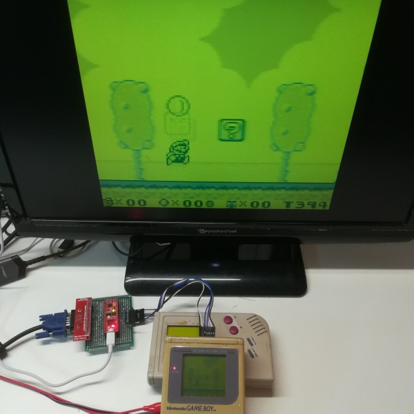
Getting the image data out of the Game Boy is surprisingly straightforward, and has been done a few times before. Basically, the connection between the CPU and the LCD screen is a serial interface with a 4 MHz clock, two data lines and two sync lines. [Martoni] uses pin headers sticking out of the Game Boy’s plastic case to connect these to a small FPGA board. The board in question is a Fireant for the VGA version and a Tang Nano 4K for the HMDI model. In either case the FPGA reads out each frame from the Game Boy’s LCD interface and draws the extracted image onto the monitor, using the same four shades of green as used on the original screen.

[Martoni] states that the ultimate goal of these projects is to make a Switch-like docking station for the original Game Boy, which is definitely something we’re looking forward to. Although adding external monitors to the Game Boy is not entirely new, we like the simplicity of this implementation and the fact that anyone can improve upon it thanks to the full source code being available. Similar hacks have been performed on the newer Game Boy Pocket and Game Boy Advance as well.

FPGA Retrocomputer: Return To Moncky

Part of the reason that retrocomputers are still so popular despite their obsolescence is that it’s possible to understand the entire inner workings of a computer like this, from the transistors all the way up to the software. Comparatively, it will likely be a long time (if ever) before anyone is building a modern computer from discrete components. To illustrate this point, plenty of 8-bit computers are available to either restore from original 80s hardware or to build from kits. And if you’d like to get even deeper into the weeds you can design your own computer including the instruction set completely from the ground up using an FPGA.

This project, called the Moncky project, is a step above the usual 8-bit computer builds as it is actually a 16-bit computer. It is built around an Arty Spartan-7 FPGA dev board running around 20 MHz and has access to 2 x 128 kB dual-port RAM for memory. To access the outside world there is a VGA output, PS/2 capability, SPI, and uses an SD card as a hard drive. This project really shines in the software, though, as the project creator [Kris Demuynck] builds everything from scratch in order to illustrate how everything works for educational purposes, and is currently working on implementing a C compiler to make programming the computer easier.

All of the project files, as well as all of the code, are available on the project’s GitHub page if you’d like to follow along or build on this homebrew 16-bit computer. It’s actually the third iteration of this computer, with the Moncky-1 and Moncky-2 being used to develop the more basic building blocks for this computer. While it’s not the first 16-bit computer we’ve seen implemented on an FPGA, it is one of the few that builds its own RISC instruction set and associated software rather than cloning a known existing processor. We’ve also seen some interesting x86 implementations on an FPGA as well.

Thanks to [koen-ieee] for the tip!

Traditional Analogue And An FPGA Make This Junkbox HF Receiver A Bit Special

We will have all at some point seen a fascinating project online, only to find not enough information to really appreciate and understand it. Such a project came [Bill Meara]’s way over at the SolderSmoke podcast, and he was fortunately able to glean more from its creator. What [Tom] had made from junkbox parts was a fairly traditional analogue receiver for the 20m amateur band which would be quite an achievement in itself, but what makes it special is its use of an FPGA to augment the analogue tuning.

A traditional analogue radio has a local oscillator which is mixed with the signal from the antenna, and an intermediate frequency of the difference between oscillator and desired signal is filtered from the result and amplified. The oscillator on older receivers would have used a free running tuned circuit, while a newer device might use a phase-locked loop to derive a stable frequency from a crystal.

What [Tom]’s receiver does is take a free-running traditional receiver and use the FPGA as a helper. It has a frequency meter that drives the display, but it also uses the measured figure to adjust the oscillator and keep it on frequency. It has two modes; while tuning it’s a traditional analogue receiver, but when left alone the FPGA stops it drifting. We like it, it’s definitely a special project.

We’ve featured a lot of radio receivers over the years, and this certainly isn’t the only one that’s a bit unconventional.

Accurate Digital Clock Keeps Ticking With FPGA

Even the most punctual among us are content to synchronize their clocks to external time sources like navigation satellite constellations, network time servers, frequency-controlled AC mains, or signals broadcast by radio stations such as WWV, CHU, and DFC77 — but not [zaphod]. After building a couple of more traditional clocks over the years, he set his sights on making a completely isolated digital clock that doesn’t rely on external synchronization (well, except to initialize the time at first power-up).

The accuracy goal he set for himself was that of a Casio F-91W wristwatch, which is specified to maintain +/- 30 seconds per month (about 12 ppm). At the heart of the design is an oven-controlled crystal oscillator whose stability is in the single-digits parts-per-billion.

The counter chain that accumulates the time is implemented in an FPGA — admittedly overkill, but [zaphod] wanted to learn FPGA programming for this project as well. An ATmega328 drives the display and does other bookkeeping tasks. The whole design is partitioned into three PCBs which fit inside a custom 3D-printed case.

[zaphod] does a thorough job documenting his build, including the bugs and failures along the way. We like the honest summary he wrote at the project’s conclusion, noting things that could be improved or should have been done differently. Be sure to check out the GitHub repository, where all the source code and PCB design files are posted. How accurate is your wristwatch, if you even wear one anymore?

Slice Your Next FPGA Design

A recent trend has been to convert high-level constructs into FPGA code like Verilog or VHDL. Silice goes the other way: it converts very hardware-specific concepts to Verilog and aims to be a more expressive and easier to use language.

Why Silice? The project’s web page enumerates its design goals:

  • A clean, simple syntax that clearly exposes the flow of operations and where clock cycles are spent.
  • Precise rules regarding flow control (loops, calls) and their clock cycle consumption.
  • Familiar hardware constructs such as always blocks, instantiation, expression tracking (wires).
  • An optional flow-control oriented design style (automatic FSM generation), that naturally integrates within a design: while, break, subroutines.
  • The possibility to easily describe pipelines.
  • Automatically takes care of creating flip-flops for variables, with automatic pruning (e.g. const or bindings).
  • Generic interfaces and grouped IOs for easy reuse and modular designs.
  • Generic circuits that can be instantiated and reused easily.
  • Explicit clock domains and reset signals.
  • Familiar syntax with both C and Verilog inspired elements.
  • Inter-operates with Verilog, allowing to import and reuse existing modules.
  • Powerful LUA-based pre-processor.

Continue reading “Slice Your Next FPGA Design”

Using Docker To Sail Through Open-Source Xilinx FPGA Development

Until a few years ago, developing for FPGAs required the use of proprietary locked-down tools, but in the last few years, the closed-source dam has burst, and open-source FPGA tools such as Yosys, SimbiFlow, and Icestorm have come flooding out. Setting up a build environment for these exciting new tools can still be quite a challenge, but [Carlos Eduardo] has decided to make setting up an open-source toolchain for Xilinx FPGAs a breeze with Docker.

His image only has three prerequisites: Docker, Python 3, and OpenOCD (which is used to load your FPGA with your bespoke bitfile). After the Docker image has been built and all of the tools installed, [Carlos] guides you through using Python, FuseSoc, and SymbiFlow to build your first open-source Xilinx FPGA project.

In addition to making setup a whole lot easier, utilizing containers allows the same development environment to be built on Linux, Mac, and Windows (using WSL), which will make life a lot easier for teams working across different OSs.  [Carlos’s] Dockerfile is unique because it supports the popular Artix-7 series of FPGAs — for the Lattice FPGAs that have been supported for a lot longer, there are existing Docker files already up on DockerHub. It’s easier than installing the vendor’s toolchain!

If this has you thinking it might be time to dip your toes into open-source FPGA development, check out this rundown of open-source FPGA tools from the 2019 Superconference.