No Acid: Open ICs With A Tesla Coil

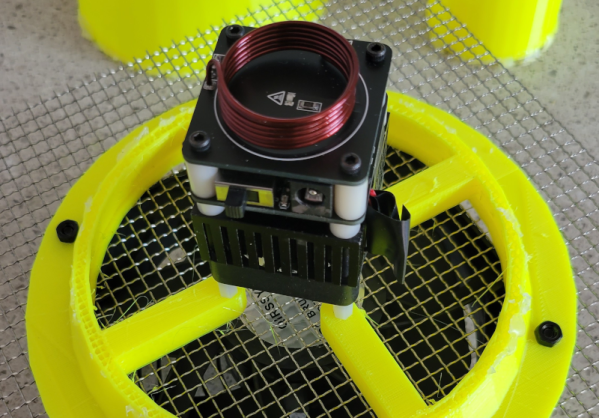
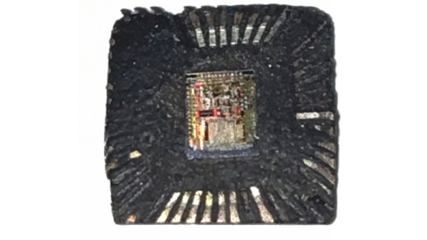
We’ve taken ICs apart before, but if they are in an epoxy package, it requires some lab gear and a lot of safety. Typically, you’ll heat the part and use fuming nitric acid (nasty stuff) in a cavity milled into the part to remove the epoxy over the die. While [100dollarhacker] doesn’t provide much detail, he appears to have used a Tesla coil to do it — no hot acid required.

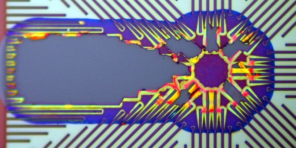
Initial results were promising but took a long time to work. In addition, the coil gets very hot, and there is a chance of flames. The next attempt used a 3D printed cone with a fan to push the plasma over the chip. The first attempt shorted something out, and so far, each attempt eventually burns out the MOSFET driver.

We are always interested in the practical uses of Tesla coils and what’s inside ICs, so this project naturally appealed to us. We hope to see more success reported on the Hackaday.io page soon. Meanwhile, if you have a coil and an old IC lying around, try it. Maybe you’ll figure out how to make it work well and if you do, let us know.

The easiest chips to open are ceramic packages with a gold lid. Just use a hobby knife. There are less noxious chemicals you can use. If you want to use fuming nitric, be sure you know what you are doing and maybe make some yourself.

Silicon Sleuthing: Finding A Ancient Bugfix On The 8086

Few CPUs have had the long-lasting influence that the 8086 did. It is hard to believe that when your modern desktop computer boots, it probably thinks it is an 8086 from 1978 until some software gooses it into a more modern state. When [Ken] was examining an 8086 die, however, he noticed that part of the die didn’t look like the rest. Turns out, Intel had a bug in the original version of the 8086. In those days you couldn’t patch the microcode. It was more like a PC board — you had to change the layout and make a new one to fix it.

The affected area is the Group Decode ROM. The area is responsible for categorizing instructions based on the type of decoding they require. While it is marked as a ROM, it is more of a programmable logic array. The bug was pretty intense. If an interrupt followed either a MOV SS or POP SS instruction, havoc ensues.

Continue reading “Silicon Sleuthing: Finding A Ancient Bugfix On The 8086”

Reverse Engineering Silicon, One Transistor At A Time

Many of will have marveled at the feats of reverse engineering achieved by decapping integrated circuits and decoding their secrets by examining the raw silicon die. Few of us will have a go for ourselves, but that doesn’t stop the process being a fascinating one. Fortunately [Ryan Cornateanu] is on hand with a step-by-step description of his journey into the art of decapping, as he takes on what might seem an unlikely subject in the form of the CH340 USB to serial chip you’ll find on an Arduino Nano board.

Starting with hot sulphuric acid is probably not everyone’s idea of a day at the bench, but having used it to strip the epoxy from the CH340, he’s able to take a look under the microscope. This is no ordinary microscope but a metallurgists instrument designed to light the top of the sample from one side with polarised light. This allows him to identify an area of mask ROM and zoom in on the transistors that make each individual bit.

At this point the chemistry moves into the downright scary as he reaches for the hydrofluoric acid and has to use a PTFE container because HF is notorious for its voracious reactivity. This allows him to take away the interconnects and look at the transistor layer. He can then with a bit of computer vision processing help extract a bit layer map, which with some experimentation and guesswork can be manipulated into a firmware dump. Even then it’s not done, because he takes us into the world of disassembly of what is an unknown architecture. Definitely worth a read for the armchair chip enthusiast.

If you’re thirsty for more, of course we have to direct you towards the work of [Ken Shirriff].

What’s Inside An FPGA? Ken Shirriff Has (Again) The Answer

FPGAs are somewhat the IPv6 of integrated circuits — they’ve been around longer than you might think, they let you do awesome things that people are intrigued by initially, but they’ve never really broke out of their niches until rather recently. There’s still a bit of a myth and mystery surrounding them, and as with any technology that has grown vastly in complexity over the years, it’s sometimes best to go back to its very beginning in order to understand it. Well, who’d be better at taking an extra close look at a chip than [Ken Shirriff], so in his latest endeavor, he reverse engineered the very first FPGA known to the world: the Xilinx XC2064.

If you ever wished for a breadboard-friendly FPGA, the XC2064 can scratch that itch, although with its modest 64 configurable logic blocks, there isn’t all that much else it can do — certainly not compared to even the smallest and cheapest of its modern successors. And that’s the beauty of this chip as a reverse engineering target, there’s nothing else than the core essence of an FPGA. After introducing the general concepts of FPGAs, [Ken] (who isn’t known to be too shy to decap a chip in order to look inside) continued in known manner with die pictures in order to map the internal components’ schematics to the actual silicon and to make sense of it all. His ultimate goal: to fully understand and dissect the XC2064’s bitstream.

Of course, reverse engineering FPGA bitstreams isn’t new, and with little doubt, building a toolchain based on its results helped to put Lattice on the map in the maker community (which they didn’t seem to value at first, but still soon enough). We probably won’t see the same happening for Xilinx, but who knows what [Ken]’s up to next, and what others will make of this.

Comparing Bare Silicon On Two Game Boy Audio Chips

We always look forward to a new blog post by [Ken Shirriff] and this latest one didn’t cure us of that. His topic this time? Comparing two Game Boy audio chips. People have noticed before that the Game Boy Color sounds very different than a classic Game Boy, and he wanted to find out why. If you know his work, you won’t be surprised to find out the comparison included stripping the die out of the IC packaging.

[Ken’s] explanation of how transistors, resistors, and capacitors appear on the die are helpfully illustrated with photomicrographs. He points out how resistors are notoriously hard to build accurately on a production IC. Many differences can affect the absolute value, so designs try not to count on exact values or, if they do, resort to things like laser trimming or other tricks.

Capacitors, however, are different. The exact value of a capacitor may be hard to guess beforehand, but the ratio of two or more capacitor values on the same chip will be very precise. This is because the dielectric — the oxide layer of the chip — will be very uniform and the photographic process controls the planar area of the capacitor plates with great precision.

We’ve decapsulated chips before, and we have to say that if you are just starting to look at chips at the die level, these big chips with bipolar transistors are much easier to deal with than the fine and dense geometries you’d find even in something like a CPU from the 1980s.

We always enjoy checking in with [Ken]. Sometime’s he’s taking apart nuclear missiles. Sometimes he is repairing an old computer. But it is always interesting.

Decap ICs Without The Peril

There can be few of us who haven’t gazed with fascination upon the work of IC decappers, whether they are showing us classic devices from the early years of mass semiconductor manufacture, or reverse-engineering the latest and greatest. But so often their work appears to require some hardcore scientific equipment or particularly dangerous chemicals. We’ve never thought we might be able to join the fun. [Generic Human] is out to change all that, by decapping chips using commonly available chemicals and easy to apply techniques. In particular, we discover through their work that rosin — the same rosin whose smell you will be familiar with from soldering flux — can be used to dissolve IC packaging.

Of course, ICs that dissolved easily in the face of soldering wouldn’t meet commercial success, so an experiment with flux meets little success. Pure rosin, however, appears to be an effective decapping agent. [Generic Human] shows us a motherboard voltage regulator boiled in the stuff. When the rosin is removed with acetone, there among the debris is the silicon die, reminding us just how tiny these things are. We’re sure you’ll all be anxious to try it for yourselves, now, so take a while to look at the video below showing their CCC Congress talk.

The master of chip decapping is of course [Ken Shirriff], whose work we’ve featured many times. Our editor [Mike Szczys] interviewed him last year, and it’s well worth a look.

Continue reading “Decap ICs Without The Peril”

A Classy SDR Chip, Decapped

If you are a regular searcher for exotic parts among the virtual pages of semiconductor supplies catalogs, you will have probably noticed that for a given function it is most often the part bearing the Analog Devices logo that is the most interesting. It may have more functionality, perhaps it will be of a higher specification, and it will certainly have a much higher price. [Zeptobars] has decapped and analyzed an AD chip that holds all three of those honors, the AD9361 SDR transceiver.

It’s placed under a slightly inflammatory title, “when microchips are more profitable than drugs“, but does make a good job of answering why a semiconductor device at the very cutting edge of what is possible at the time of release can be so expensive. The AD9361 is an all-in-one SDR transceiver with an astonishing bandwidth, and as such was a particularly special device when it reached the market in 2013. We see some particularly fine examples of on-chip inductors and PLL circuitry that must have consumed a significant design effort to preserve both bandwidth and noise characteristics. This is an item of physical beauty at a microscopic scale as well as one of technical achievement.

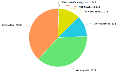
The financial analysis puts Analog Devices’s gross profit at about $103 of the $275 retail purchase price of an AD9361. The biggest slice at $105 goes to the distributor, and surprisingly the R&D and manufacturing costs are not as large as you might expect. How accurate these figures are is anybody’s guess, but they are derived from an R&D figure in the published financial report, so there is some credence to be given to them.

We’ve featured [Zeptobar’s] work before more than once. A look at fake Nordic Semi parts for example or a Soviet i8080 clone have received their treatment. Always a source to watch out for!