Exploring Early ’90s Video Game Architecture With Another World

Curious about past computer architectures? Software engineer [Fabien Sanglard] has been experimenting with porting Another World, an action-adventure platformer, to different machines and comparing the results in his “Polygons of Another World” project.

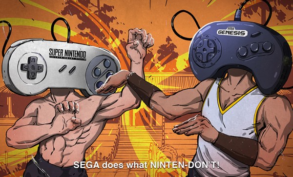
The results are pretty interesting. Due to the game’s polygon-based graphics, optimizations vary widely across different architectures, with tricks allowing the software to run on hardware released five years before the game’s publication. The consoles explored are primarily from the early ’90s, ranging from the Amiga 500, Atari ST, IBM PC, and Super Nintendo to the Sega Genesis.

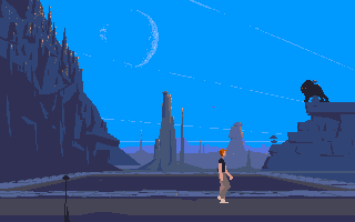
The actual game contains very little code, with the original version at 6000 lines of assembly and the PC DOS executable only containing 20 KiB. The executable simply exists as a virtual machine host that reads and executes uint8_t opcodes, with most of the business logic implemented with bytecode. The graphics use 16 palette-based colors, despite the Amiga 500 supporting up to 32 colors. However, the aesthetics still fit the game nicely, with some very pleasant pixel art.

There’s a plethora of cool tricks that emerge in each of the ports, starting with the original Amiga 500 execution. Prior to the existence of the CPU/GPU architecture, microprocessors had blitters – logic blocks that rapidly modified data within the memory, capable of copying large swathes of data in parallel with the CPU, freeing up the CPU for other operations.

To display the visuals, a framebuffer containing a bitmap drives the display. There are three framebuffers used, two for double buffering and one for saving the background composition to avoid redrawing static polygons. Within the framebuffer, several tricks are used to improve the graphical experience. For scenes with translucent hues, special values are interpreted from the framebuffer index by “reading the framebuffer index, adding 0x8 and writing back”.

Challenges also come when manipulating pixels given each machine’s CPU and bus bandwidth limitations. For filling in bits, the blitter uses a feature called “Area Fill Mode” that scans left to right to find edges, rendering the bit arrays with spaces between lines filled in. Since the framebuffer is stored in five separate areas of memory – or bitplanes – this requires drawing the lines and filling in areas four times, multiplying by the hundreds of polygons rendered by the engine. The solution was to set up a temporary “scratchpad” buffer and rendering a polygon into the clean space. The polygon can then get copied to the screen area with a masked blit operation since the blitter can render anywhere in memory.

Intrigued? The series continues with deep dives into Atari ST, IBM PC, and upcoming writeups on SEGA Genesis/MegaDrive.

The Golden Age Of Ever-Changing Computer Architecture

Given the accuracy of Moore’s Law to the development of integrated circuits over the years, one would think that our present day period is no different from the past decades in terms of computer architecture design. However, during the 2017 ACM Turing Award acceptance speech, John L. Hennessy and David A. Patterson described the present as the “golden age of computer architecture”.

Compared to the early days of MS-DOS, when designing user- and kernel-space interactions was still an experiment in the works, it certainly feels like we’re no longer in the infancy of the field. Yet, as the pressure mounts for companies to acquire more computational resources for running expensive machine learning algorithms on massive swaths of data, smart computer architecture design may be just what the industry needs.

Moore’s law predicts the doubling of transistors in an IC, it doesn’t predict the path that IC design will take. When that observation was made in 1965 it was difficult or even impossible to envision where we are today, with tools and processes so closely linked and widely available that the way we conceive processor design is itself multiplying.

Continue reading “The Golden Age Of Ever-Changing Computer Architecture”

Winning The Console Wars – An In-Depth Architectural Study

From time to time, we at Hackaday like to publish a few engineering war stories – the tales of bravery and intrigue in getting a product to market, getting a product cancelled, and why one technology won out over another. Today’s war story is from the most brutal and savage conflicts of our time, the console wars.

The thing most people don’t realize about the console wars is that it was never really about the consoles at all. While the war was divided along the Genesis / Mega Drive and the Super Nintendo fronts, the battles were between games. Mortal Kombat was a bloody battle, but in the end, Sega won that one. The 3D graphics campaign was hard, and the Starfox offensive would be compared to the Desert Fox’s success at the Kasserine Pass. In either case, only Sega’s 32X and the British 7th Armoured Division entering Tunis would bring hostilities to an end.

In any event, these pitched battles are consigned to be interpreted and reinterpreted by historians evermore. I can only offer my war story of the console wars, and that means a deconstruction of the hardware.

Continue reading “Winning The Console Wars – An In-Depth Architectural Study”

RISC, Tagged Memory, And Minion Cores

Buy a computing device nowadays, and you’re probably getting something that knows x86 or an ARM. There’s more than one architecture out there for general purpose computing with dual-core MIPS boards available and some very strange silicon that’s making its way into dev boards. lowRISC is the latest endeavour from a few notable silicon designers, able to run Linux ‘well’ and adding a few novel security features that haven’t yet been put together this way before.

There are two interesting features that make the lowRISC notable. The first is tagged memory. This has been used before in older, weirder computers as a sort of metadata for memory. Basically, a few bits of each memory address tag each memory address as executable/non-executable, serve as memory watchpoints, garbage collection, and a lock on every word. New instructions are added to the ISA, allowing these tags to be manipulated, watched, and monitored to prevent the most common single security problem: buffer overflows. It’s an extremely interesting application of tagged memory, and something that isn’t really found in a modern architecture.

The second neat feature of the lowRISC are the minions. These are programmable devices tied to the processor’s I/O that work a lot like a Zynq SOC or the PRU inside the BeagleBone. Basically, they’re used for programmable I/O, implementing SPI/I2C/I2S/SDIO in software, offloading work from the main core, and devices that require very precise timing.

The current goal of the lowRISC team is to develop the hardware on an FPGA, releasing some beta silicon in a year’s time. The first complete chip will be an embedded SOC, hopefully release sometime around late 2016 or early 2017. The ultimate goal is an SOC with a GPU that would be used in mobile phones, set-top boxes, and Raspi and BeagleBone-like dev boards. There are enough people on the team, including [Robert Mullins] and [Alex Bradbury] of the University of Cambridge and the Raspberry Pi, researchers at UC Berkeley, and [Bunnie Huang].

It’s a project still in its infancy, but the features these people are going after are very interesting, and something that just isn’t being done with other platforms.

[Alex Bardbury] gave a talk on lowRISC at ORConf last October. You can check out the presentation here.

Building New, Weird CPUs In FPGAs

CPU

The popularization of FPGAs for the hobbyist market means a lot more than custom LED controllers and clones of classic computer systems. FPGAs are also a great tool to experiment with computer architecture, creating new, weird, CPUs that don’t abide by the conventions the industry has used for 40 years. [Victor] is designing a new CPU that challenges the conventions of how to access different memory locations, and in the process even came up with a bit of example code that runs on an ARM microcontroller.

Most of the time, the machine code running on your desktop or laptop isn’t that interesting; it’s just long strings of instructions to be processed linearly. The magic of a computer comes through comparisons, an if statement or a jump in code, where the CPU can run one of two pieces of code, depending on a value in a register. There is the problem of reach, though: if a piece of code makes a direct call to another piece of code, the address of the new code must fit within an instruction. On an ARM processor, only 24 bits are available to encode the address, meaning a jump in code can only go 16 MB on either side of its call. Going any further requires more instructions, and the performance hit that comes along with that.

[Victor] decided a solution to this problem would be to create a bit of circuitry that would be a sliding window to store address locations. Instead of storing the literal address for jumps in code, every branch in the code is stored as a location relative to whatever is in the program counter. The result is an easy way to JMP to code very far away in memory, with less of a performance hit.

There’s an implementation for this sliding window token thing [Victor] whipped up for NXP’s ARM Cortex M3 microprocessor, and he’ll be working on an implementation of this concept in a new CPU over on his git.

Massively Parallel CPU Processes 256 Shades Of Gray

256

The 1980s were a heyday for strange computer architectures; instead of the von Neumann architecture you’d find in one of today’s desktop computers or the Harvard architecture of a microcontroller, a lot of companies experimented with strange parallel designs. While not used much today, at the time these were some of the most powerful computers of their day and were used as the main research tools of the AI renaissance of the 1980s.

Over at the Norwegian University of Science and Technology a huge group of students (13 members!) designed a modern take on the massively parallel computer. It’s called 256 Shades of Gray, and it processes 320×240 pixel 8-bit grayscale graphics like no microcontroller could.

The idea for the project was to create an array-based parallel image processor with an architecture similar to the Goodyear MPP formerly used by NASA or the Connection Machine found in the control room of Jurassic Park. Unlike these earlier computers, the team implemented their array processor in an FPGA, giving rise to their Lena processor this processor is in turn controlled by a 32-bit AVR microcontroller with a custom-build VGA output.

The entire machine can process 10 frames per second of 320×240 resolution grayscale video. There’s a presentation video available (in Norwegian), but the highlight might be their demo of The Game of Life rendered in real-time on their computer. An awesome build, and a very cool experience for all the members of the class.