Learn IC Decapping

Decapsulating ICs used to be an exotic technique. (I should know, I did that professionally for one of the big IC vendors back in the 1980s.) These days, more and more people are learning to take apart ICs for a variety of reasons. If you are interested in doing it yourself, [Juan Carlos Jimenez] has a post you should read about using acid to remove epoxy from ICs.

[Juan Carlos] used several different techniques with varying degrees of success. Keep in mind, that using nitric acid is generally pretty nasty. You need safety equipment and be sure to plan for bad things to happen. Have eyewash ready because once you splash acid in your eye, it is too late to get that together.

Continue reading “Learn IC Decapping”

What’s Inside An FPGA? Ken Shirriff Has (Again) The Answer

FPGAs are somewhat the IPv6 of integrated circuits — they’ve been around longer than you might think, they let you do awesome things that people are intrigued by initially, but they’ve never really broke out of their niches until rather recently. There’s still a bit of a myth and mystery surrounding them, and as with any technology that has grown vastly in complexity over the years, it’s sometimes best to go back to its very beginning in order to understand it. Well, who’d be better at taking an extra close look at a chip than [Ken Shirriff], so in his latest endeavor, he reverse engineered the very first FPGA known to the world: the Xilinx XC2064.

If you ever wished for a breadboard-friendly FPGA, the XC2064 can scratch that itch, although with its modest 64 configurable logic blocks, there isn’t all that much else it can do — certainly not compared to even the smallest and cheapest of its modern successors. And that’s the beauty of this chip as a reverse engineering target, there’s nothing else than the core essence of an FPGA. After introducing the general concepts of FPGAs, [Ken] (who isn’t known to be too shy to decap a chip in order to look inside) continued in known manner with die pictures in order to map the internal components’ schematics to the actual silicon and to make sense of it all. His ultimate goal: to fully understand and dissect the XC2064’s bitstream.

Of course, reverse engineering FPGA bitstreams isn’t new, and with little doubt, building a toolchain based on its results helped to put Lattice on the map in the maker community (which they didn’t seem to value at first, but still soon enough). We probably won’t see the same happening for Xilinx, but who knows what [Ken]’s up to next, and what others will make of this.

Deep-Sleep Problems Lead To Forensic Investigation Of Troublesome Chip

When you buy a chip, how can you be sure you’re getting what you paid for? After all, it’s just a black fleck of plastic with some leads sticking out of it, and a few laser-etched markings on it that attest to what lies within. All of that’s straightforward to fake, of course, and it’s pretty easy to tell if you’ve got a defective chip once you try it out in a circuit.

But what about off-brand chips? Those chips might be functionally similar, but still off-spec in some critical way. That was the case for [Kevin Darrah] which led to his forensic analysis of potentially counterfeit MCU chips. [Kevin] noticed that one of his ATMega328 projects was consuming way too much power in deep sleep mode — about two orders of magnitude too much. The first video below shows his initial investigation and characterization of the problem, including removal of the questionable chip from the dev board it was on and putting it onto a breakout board that should draw less than a microamp in deep sleep. Showing that it drew 100 μA instead sealed the deal — something was up with the chip.

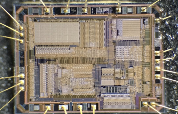
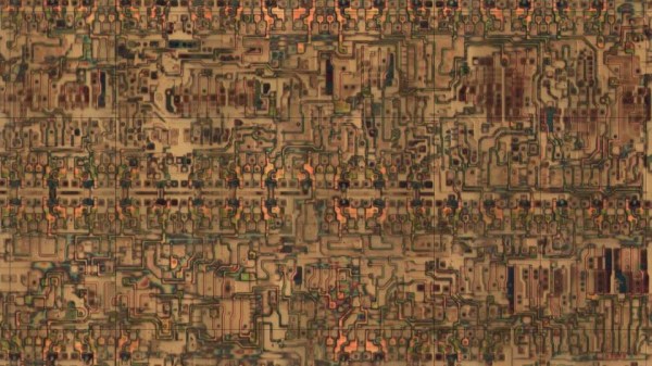
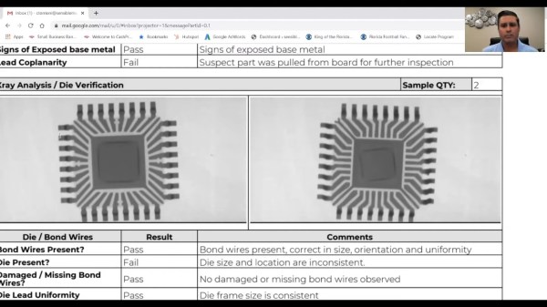
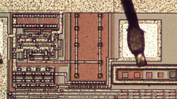
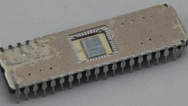
[Kevin] then sent the potentially bogus chip off to a lab for a full forensic analysis, because of course there are companies that do this for a living. The second video below shows the external inspection, which revealed nothing conclusive, followed by an X-ray analysis. That revealed enough weirdness to warrant destructive testing, which showed the sorry truth — the die in the suspect unit was vastly different from the Atmel chip’s die.

It’s hard to say that this chip is a counterfeit; after all, Atmel may have some sort of contract with another foundry to produce MCUs. But it’s clearly an issue to keep in mind when buying bargain-basement chips, especially ones that test functionally almost-sorta in-spec. Caveat emptor.

Counterfeit parts are depressingly common, and are a subject we’ve touched on many times before. If you’d like to know more, start with a guide.

Continue reading “Deep-Sleep Problems Lead To Forensic Investigation Of Troublesome Chip”

Hackaday Links Column Banner

Hackaday Links: September 13, 2020

Like pretty much every other big conference, the Chaos Communication Conference is going virtual this year. What was supposed to be 37C3 has been rebranded as rC3, the remote Chaos Experience. It’s understandable, as a 17,000 person live event would have not only been illegal but a bit irresponsible in the current environment. The event appears to be a hybrid of small local events hosted in hackerspaces linked with streamed talks and a program of workshops and “online togetherness.” rC3 is slated to run in the week between Christmas and New Year, and it seems like a great way to wrap up 2020.

Speaking of remote conferences, don’t forget about our own Remoticon. While it won’t be quite the same as everyone getting together in sunny — historically, at least — Pasadena for a weekend of actual togetherness, it’s still going to be a great time. The event runs November 6 to 8; we’ve had a sneak peek at the list of proposed workshops and there’s some really cool stuff. Prepare to be dazzled, and make sure you keep up on the Remoticon announcements — you really don’t want to miss this.

Continue reading “Hackaday Links: September 13, 2020”

Reverse Engineering The Charge Pump Of An 8086 Microprocessor

You’d think that the 8086 microprocessor, a 40-year-old chip with a mere 29,000 transistors on board that kicked off the 16-bit PC revolution, would have no more tales left to tell. But as [Ken Shirriff] discovered, reverse engineering the chip from die photos reveals some hidden depths.

The focus of [Ken]’s exploration of the venerable chip is the charge pump, a circuit that he explains was used to provide a bias voltage across the substrate of the chip. Early chips generally took this -5 volt bias voltage from a pin, which meant designers had to provide a bipolar power supply. To reduce the engineering effort needed to incorporate the 8086 into designs, Intel opted for an on-board charge pump to generate the bias voltage. The circuit consists of a ring oscillator made from a trio of inverters, a pair of transistors, and some diodes to act as check valves. By alternately charging a capacitor and switching its polarity relative to the substrate, the needed -5 volt bias is created.

Given the circuit required, it was pretty easy for [Ken] to locate it on the die. The charge pump takes up a relatively huge amount of die space, which speaks to the engineering decisions Intel made when deciding to include it. [Ken] drills down to a very low level on the circuit, with fascinating details on how the MOSFETs were constructed, and why eight transistors were used instead of two diodes. As usual, his die photos are top quality, as are his explanations of what’s going on down inside the silicon.

If you’re somehow just stumbling upon [Ken]’s body of work, you’re in for a real treat. To get you started, you’ll want to check out how he found pi baked into the silicon of the 8087 coprocessor, or perhaps his die-level exploration of different Game Boy audio chips.

Looking For Pi In The 8087 Math Coprocessor Chip

Even with ten fingers to work with, math can be hard. Microprocessors, with the silicon equivalent of just two fingers, can have an even harder time with calculations, often taking multiple machine cycles to figure out something as simple as pi. And so 40 years ago, Intel decided to give its fledgling microprocessors a break by introducing the 8087 floating-point coprocessor.

If you’ve ever wondered what was going on inside the 8087, wonder no more. [Ken Shirriff] has decapped an 8087 to reveal its inner structure, which turns out to be closely related to its function. After a quick tour of the general layout of the die, including locating the microcode engine and ROM, and a quick review of the NMOS architecture of the four-decade-old technology, [Ken] dug into the meat of the coprocessor and the reason it could speed up certain floating-point calculations by up to 100-fold. A generous portion of the complex die is devoted to a ROM that does nothing but store constants needed for its calculation algorithms. By carefully examining the pattern of NMOS transistors in the ROM area and making some educated guesses, he was able to see the binary representation of constants such as pi and the square root of two. There’s also an extensive series of arctangent and log2 constants, used for the CORDIC algorithm, which reduces otherwise complex transcendental calculations to a few quick and easy bitwise shifts and adds.

[Ken] has popped the hood on a lot of chips before, finding butterflies in an op-amp and reverse-engineering a Sinclair scientific calculator. But there’s something about seeing constants hard-coded in silicon that really fascinates us.

Chip Decapping The Easy Way

Chip decapping videos are a staple of the hacking world, and few things compare to the beauty of a silicon die stripped of its protective epoxy and photographed through a good microscope. But the process of actually opening that black resin treasure chest seems elusive, requiring as it does a witch’s brew of solvents and acids.

Or does it? As [Curious Marc] documents in the video below, a little heat and some finesse are all it takes, at least for some chips. The method is demonstrated by [Antoine Bercovici], a paleobotanist who sidelines as a collector of old chips. After removing chips from a PCB — he harvested these chips from an old PlayStation — he uses hot air to soften the epoxy, and then flexes the chip with a couple of pairs of pliers. It’s a bit brutal, but in most of the Sony chips he tried for the video, the epoxy broke cleanly over the die and formed a cleavage plane that allowed the die to be slipped out cleanly. The process is not unlike revealing fossils in sedimentary rocks, a process that he’s familiar with from his day job.

He does warn that certain manufacturers, like Motorola and National, use resins that tend to stick to the die more. It’s also clear that a hairdryer doesn’t deliver enough heat; when they switched to a hot air rework station, the success rate went way up.

The simplicity of this method should open the decapping hobby up to more people. Whether you just want to take pretty pictures or if reverse engineering is on your mind, put the white fuming nitric acid down and grab the heat gun instead.

Continue reading “Chip Decapping The Easy Way”