Semi-Auto PCB Drill Press Makes Drilling Semi-Painless

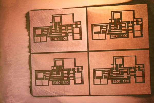
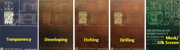
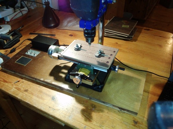
DIY PCBs are the fastest and cheapest way to iteratively prototype circuits, and there’s a lot of great tricks to get the copper layer just the way you want it. But if you’re using through-hole parts, you eventually have to suffer the tedium of drilling a potentially large number of precisely aligned holes. Until now. [Acidbourbon] has built up a very nice semi-automatic PCB drill machine.

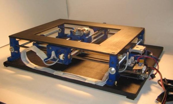
Semi-automatic? The CNC machine (with PC-side software) parses the drill file that most PCB design software spits out, and moves an X-Y table under your drill press to just the right spots. The user manually drills the hole and hits enter, and the table scoots off to the next drilling location. All of this is tied together with a simple calibration procedure that figures out where you’ve got the board using two reference drill locations; you initially jog the platform to two reference drill holes, and you’re set.

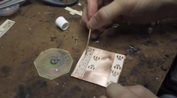
The CNC conversion of a relatively cheap X-Y table is nicely documented, and the on-board touchscreen and USB interface seem to make driving the machine around painless. Or at least a lot less painful than aligning up and drilling all the holes the old-fashioned way. Everything is open-source, so head on over and check it out.  (And while you’re there, don’t miss [Acidbourbon]’s tips and tricks for making PCBs using the toner transfer method.)

Seeing this machine in action, we can’t wait for the fully automatic version.

Continue reading “Semi-Auto PCB Drill Press Makes Drilling Semi-Painless”

PCB Laser Printer

PCB Toner Transfer Method, Now Without The Transfer

A common way to create a custom PCB at home is to do what is called the Toner Transfer Method. In this process, the trace layout of the board is printed out on a piece of special toner transfer paper that allows the ink to come off in the following step. The toner transfer paper is then put print-side-down on a copper clad PCB blank, heated and pressed with an iron. The heat and pressure from the iron transfers the toner from the paper to the copper. The exposed copper then is chemically removed, the previously applied toner protects the copper in the pad and trace areas. The toner is then removed using paint thinner.

That is a long process with many critical steps. [mlerman] wondered why no one was printing the toner directly to the PCB. He has been tinkering with printing directly on PCB blanks for 4 years now. He’s made hundreds of boards over that time and can now make a PCB in under 15 minutes.

The obvious route to take would be to modify a current laser printer to accept the much-thicker-than-paper PCB boards. A few printer models were tried but [mlerman] feels the Lexmark E260 works the best due to the cost, internal mechanical components and an easily modifiable manual feed system. There is also a Local Printer Utility that allows the majority of the printer parameters to be adjusted.

Continue reading “PCB Toner Transfer Method, Now Without The Transfer”

DIY Circuit Boards Look Professional

Professional Looking DIY PCB Boards

Making PCBs at home is a great means to get your prototype up and running without having to wait weeks for a professionally made board. Regardless if these prototype boards are milled or etched, they are easily identified as ‘home brew’ due to their ‘unfinished’ appearance. [HomeDIY&Stuff] has put together a little how-to on the process for making DIY PCBs look a little closer to a professionally manufactured board.

The process starts out with designing the board in a PCB program. There are a lot of these programs available. Eagle is a popular choice and has a free version available. Once the layout it finalized, the design is printed out on a transparent sheet of plastic. A blank copper-clad PCB board that already has a UV sensitive coating applied are available for purchase and is what is used in this example. The transparency is placed over the PCB blank and then exposed to UV light. The coating on the PCB cures where ever the UV light passes through the open areas of the transparency.

Once the transparency is removed, there is a noticeable difference in coating color where it has cured. This board is now placed in a developer solution that removes the un-cured UV sensitive coating. A Ferric Chloride acid bath then etches away at the now-exposed copper. The cured coating from the previous step protects the copper at the trace locations during the etch process. The result is a board with copper where you want it and none where you don’t. If the board has any through-hole components, this would be the time to drill those holes.

Up to this point the process has been pretty standard for homemade PCBs and the next part is certainly the most interesting but, unfortunately, is also the worst documented step; the solder mask and silk screening. It appears that two silk screens are produced, one for the solder mask and one for the silk screen. The artwork for making the silk screens can be output from the PCB design software. There is no mention of the solder mask material used but oil-based silk screen ink is specified. Although the details are lacking, the photos show that it works pretty well. If you have had any experience with silk screening DIY PCBs, let us know in the comments.

Cheap, Resourceful DIY Mini CNC Router/Mill Contraption

Few Hackaday Readers would disagree with the classic phrase: Necessity is the mother of invention. That statement is certainly no exaggeration when it comes to this mini 3-axis CNC Machine. The builder, [Jonathan], needed a way to prototype circuit boards that he designed. And although he admittedly doesn’t use it as much as he intended, the journey is one of invention and problem solving.

[Jonathan] started from the ground up with his own design. His first machine was a moving gantry style (work piece doesn’t move) and ended up not performing to his expectations. The main problem was alignment of the axis rails. Not becoming discouraged, [Jonathan] started on version 2. This time around the work piece would move in the X and Y directions like a conventional vertical milling machine. The Porter-Cable laminate trimmer would move up and down for the Z axis. It is clear that the frame is built specifically for this project. Although not the prettiest, the frame is completely functional and satisfactorily stiff for what it needs to do.

Continue reading “Cheap, Resourceful DIY Mini CNC Router/Mill Contraption”

Laser-Based PCB Printer

Being able to create PCB’s at home is a milestone in the DIYer’s arsenal. Whether you physically mill or chemically etch boards, it’s a tricky task to perfect. [Charlie & Victor] are working towards a solution to this complicated chore. They call their machine the DiyouPCB. DiyouPCB is an open source PCB etching project consisting of both hardware and software components.

The project is based on using a Blue Ray optical pickup. The pickup was used in its entirety, without any modification, to simplify the build process. In order to use the stock pickup, [Charlie & Victor] had to reverse engineer the communication protocol which also allowed them to take advantage of the auto-focus feature used while reading Blue Ray discs. The frame of the machine is reminiscent of a RepRap, which they used to do preliminary testing and laser tuning. The X and Y axes run on brass bushings and are belt driven by stepper motors which are controlled by an Arduino through a specially designed DiyouPCB Controller Shield.

Continue reading “Laser-Based PCB Printer”

DIY Heatsinking PCBs

pcb heatsink

We have covered many do it yourself PCBs before, but this video guide adds an easy way to sink heat from high power devices, which we think you might find handy.

It is a very simple process that [CNLohr] uses to keep his small RGB LED projects from overheating. It starts by using a readily available silicone thermal sheet as the substrate by applying it to copper foil. He then applies a toner-transfer circuit pattern to the copper by running the pair through a modified laminator a few times. He makes note that you have to apply the plastic backing side of the silicone sheet to the copper foil to prevent the laminator from chewing it up.

After the typical ferric chloride etching process is complete, he then uses 220 grit sandpaper to remove the toner pattern. Often steel wool is used, but because of the sensitive nature of the silicone, sandpaper works better to avoid peeling up traces.

We have featured [CNLohr] before, as he does some top-notch tutorials in his workshop — which makes for both a fascinating and distracting backdrop for the videos. This one is a bit long (~20 minutes), but is very thorough and goes through the entire process from start to finish. Check it out after the break.

Continue reading “DIY Heatsinking PCBs”

How-to: Prepare Your Eagle Designs For Manufacture

back

Cadsoft Eagle is a multi-platform freeware circuit layout program. Lots of open source hardware is designed in Eagle, and it’s become a hobbyist favorite. We use it for all of our hardware designs.

There are several ways to turn an Eagle design into an actual printed circuit board (PCB). We’ll show you how to save Eagle designs as industry-standard gerber files that are accepted by any PCB manufacturer. You can use the gerbers to order a single prototype, or a full panel.

Continue reading “How-to: Prepare Your Eagle Designs For Manufacture”