Printing, Plating, And Baking Makes DIY Microlattices Possible

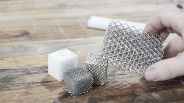
To be honest, we originally considered throwing [Zachary Tong]’s experiments with ultralight metallic microlattices into the “Fail of the Week” bucket. But after watching the video below for a second time, it’s just not fair to call this a fail, so maybe we’ll come up with a new category — “Qualified Success of the Week”, perhaps?

[Zachary]’s foray into the strange world of microlattices began when he happened upon a 2011 paper on the subject in Science. By using a special photocurable resin, the researchers were able to use light shining through a mask with fine holes to create a plastic lattice, which was then plated with nickel using the electroless process, similar to the first half of the electroless nickel immersion gold (ENIG) process used for PCBs. After removing the resin with a concentrated base solution, the resulting microlattice is strong, stiff, and incredibly light.

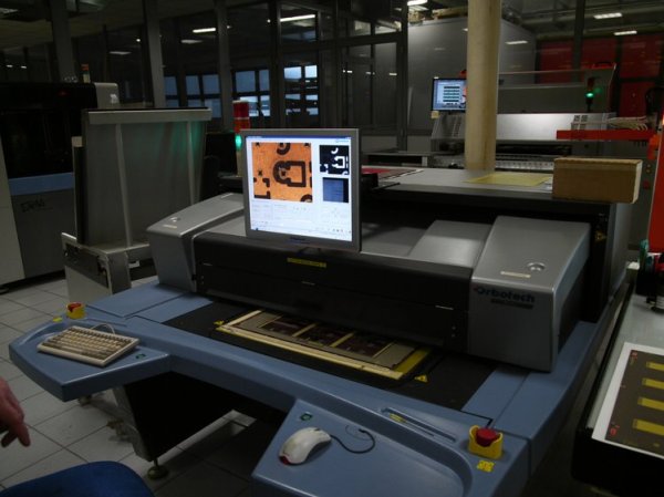
Lacking access to the advanced materials and methods originally used, [Zachary] did the best he could with what he had. An SLA printer with off-the-shelf resin was used to print the skeleton using the same algorithms used in the original paper. Those actually turned out pretty decent, but rather than electroless plating, he had to go with standard electroplating after a coat of graphite paint. The plated skeletons looked great — until he tried to dissolve the resin. When chemical approaches failed, into the oven went the plated prints. Sadly, it turns out that the polymers in the resin expand when heated, which blew the plating apart. A skeleton in PLA printed on an FDM printer fared little better; when heated to drive out the plastic, it became clear that the tortuous interior of the lattice didn’t plate very well.

From aerogels to graphene, we love these DIY explorations of new and exotic materials, so hats off to [Zachary] for giving it a try in the first place.

Continue reading “Printing, Plating, And Baking Makes DIY Microlattices Possible”

Hackaday Links Column Banner

Hackaday Links: April 5, 2020

Git is powerful, but with great power comes the ability to really bork things up. When you find yourself looking at an inscrutable error message after an ill-advised late-night commit, it can be a maximum pucker-factor moment, and keeping a clear enough head to fix the problem can be challenging. A little proactive social engineering may be in order, which is why Jonathan Bisson wrote git-undo, a simple shell script that displays the most common un-borking commands he’s likely to need. There are other ways to prompt yourself through Git emergencies, like Oh Shit, Git (or for the scatologically sensitive, Dangit Git), but git-undo has the advantage of working without an Internet connection.

Suddenly find yourself with a bunch of time on your hands and nothing to challenge your skills? Why not try to write a program in a single Tweet? The brainchild of Dominic Pajak, the BBC Micro Bot Twitter account accepts tweets and attempts to run them as BASIC programs on a BBC Microcomputer emulator, replying with the results of the program. It would seem that 280 characters would make it difficult to do anything interesting, but check out some of the results. Most are graphic displays, some animated, and with an unsurprising number of nods to 1980s pop culture. Some are truly impressive, though, like Conway’s Game of Life written by none other than Eben Upton.

The COVID-19 pandemic is causing all sorts of cultural shifts, but we didn’t expect to see much change in the culture of a community that’s been notoriously resistant to change for over a century: amateur radio. One of the most basic facts of life in the amateur radio world is that you need a license to participate, with governments regulating the process. But as a response to the pandemic, Spain has temporarily lifted licensing requirements for amateur radio operators. Normally, an unlicensed person is only allowed to operate on amateur bands under the direct supervision of a licensed amateur. The rules change allows unlicensed operators to use a station without supervision and is intended to give schoolchildren trapped at home an educational experience. In another change, some countries are allowing special callsign suffixes, like “STAYHOME,” to raise awareness during the pandemic. And the boom in interest in amateur radio since the pandemic started is remarkable; unfortunately, finding a way to take your test in a socially distant world is quite a trick. Our friend Josh Nass (KI6NAZ) has some thoughts about testing under these conditions that you might find interesting.

And finally, life goes on during all this societal disruption, and every new life deserves to be celebrated. And when Lauren Devinck made her appearance last month, her proud parents decided to send out unique birth announcement cards with a printed circuit board feature. The board is decorative, not functional, but adds a distinctive look to the card. The process of getting the boards printed was non-trivial; it turns out that free-form script won’t pass most design rule tests, and that panelizing them required making some compromises. We think the finished product is classy, but can’t help but think that a functional board would have really made a statement. Regardless, we welcome Lauren and congratulate her proud parents.

PCB Finishes Hack Chat

Join us on Wednesday, March 11 at noon Pacific for the PCB Finishes Hack Chat with Mark Hughes and Elijah Gracia!

There’s no way to overestimate the degree to which the invention of the printed circuit board revolutionized electronics. What was once the work of craftspeople weaving circuits together with discrete components, terminal strips, and wiring harnesses could now be accomplished with dedicated machines, making circuit construction an almost human-free process. And it was all made possible by figuring out how to make copper foil stick to a flat board, and how to remove some of it while leaving the rest behind.

​Once those traces are formed, however, there’s more work to be done. Bare copper is famously reactive stuff, and oxides soon form that will make the traces difficult to solder later. There are hundreds of different ways to prevent this, and PCB surface finishing has become almost an art form itself. Depending on the requirements for the circuit, traces can be coated with tin, lead, gold, nickel, or any combination of the above, using processes ranging from electroplating to immersion in chemical baths. And the traces aren’t the only finishes; solder resist and silkscreening are both important to the usability and durability of the finished board.

For this Hack Chat, we’ll be talking to Elijah Gracia and Mark Hughes from Royal Circuit Solutions. They’re both intimately familiar with the full range of PCB coatings and treatments, and they’ll help us make sense of the alphabet soup​: HASL, OSP, ENIG, IAg, LPI, and the rest. We’ll learn what the different finishes do, which to choose under what circumstances, and perhaps even learn a bit about how to make our homebrew boards look a little more professional and perform a bit better.

join-hack-chatOur Hack Chats are live community events in the Hackaday.io Hack Chat group messaging. This week we’ll be sitting down on Wednesday, March 11 at 12:00 PM Pacific time. If time zones have got you down, we have a handy time zone converter.

Click that speech bubble to the right, and you’ll be taken directly to the Hack Chat group on Hackaday.io. You don’t have to wait until Wednesday; join whenever you want and you can see what the community is talking about.

PCB Take On Stars, Moons, And Ringed Planets Is Gold

Remember when PCBs were green and square? That’s the easy default, but most will agree that when you’re going to show off your boards instead of hiding them in a case, it’s worth extra effort to make them beautiful. We’re in a renaissance of circuit board design and the amount of effort being poured into great looking boards is incredible. The good news is that this project proves you don’t have to go nuts to achieve great results. This stars, moons, and planets badge looks superb using just two technical tricks: exposed (plated) copper and non-rectangular board outline.

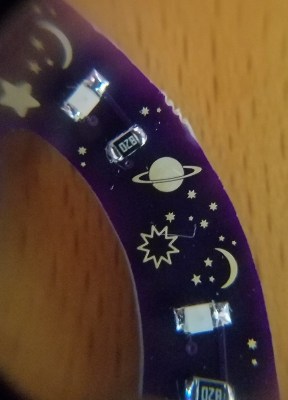
Don’t take that the wrong way, there’s still a lot of creativity that [Steve] over at Big Mess o’ Wires used to make it look this great. The key element here is that copper and solder mask placements have extremely fine pitch. After placing the LEDs and resistors there’s a lot of blank space which was filled with what you might see in the night sky through your telescope.  What caught our eye about this badge is the fidelity of the ringed planet.

The white ink of silk screen is often spotty and jagged at the edges. But this copper with ENIG (gold) plating is crisp through the curves and with razor-sharp tolerance. It’s shown here taken under 10x magnification and still holds up. This is a trick to keep under your belt — if you have ground pours it’s easy to spice up the look of your boards just by adding negative-space art in the solder mask!

[Steve] mentions the board outline is technically not a circle but “a many-sided polygon” due to quirks of Eagle. You could have fooled us! We do like how he carried the circle’s edges through the bulk of the board using silk screen. If you’re looking for tips on board outline and using multiple layers of art in Eagle, [Brian Benchoff] published a fabulous How to do PCB art in Eagle article. Of course, he’s gone deeper than what the board houses offer by grabbing his own pad printing equipment and adding color to white solder mask.

The art was the jumping off point for featuring this badge, but [Steve] is known for his technical dives and this one is no different. He’s done a great job of recounting everything that popped up while designing the circuit, from LED color choice to coin cell internal resistance and PWM to low-power AVR tricks.

A Automated Optical Inspection machine, inspecting the USB Armory board

Meet The Machines That Build Complex PCBs

You can etch a simple PCB at home with a few chemicals and some patience. However, once you get to multilayer boards, you’re going to want to pay someone to do the dirty work.

The folks behind the USB Armory project visited the factories that build their 6 layer PCB and assemble their final product. Then they posted a full walkthrough of the machines used in the manufacturing process.

The boards start out as layers of copper laminates. Each one is etched by applying a film, using a laser to print the design from a Gerber file, and etching away the unwanted copper in a solution. Then the copper and fibreglass prepreg sandwich is bonded together with epoxy and a big press.

Bonded boards then get drilled for vias, run through plating and solder mask processes and finally plated using an Electroless Nickel Immersion Gold (ENIG) process to give them that shiny gold finish. These completed boards are shipped off to another company, where a pick and place followed by reflow soldering mounts all the components to the board. An X-Ray is used to verify that the BGA parts are soldered correctly.

The walkthrough gives a detailed explanation of the process. It shows us the machines that create products we rely on daily, but never get to see.