World’s Smallest Comic Etched Onto A Human Hair

world's smallest comic

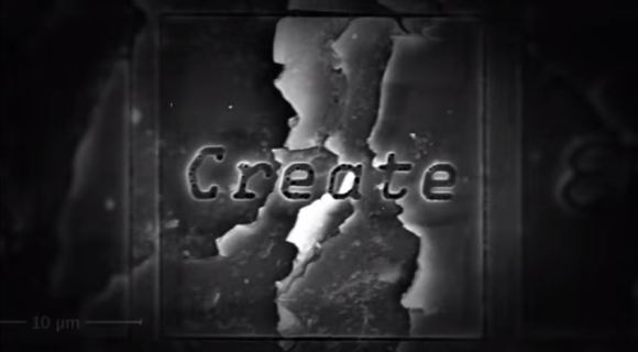
[Sébastien Bourdeauducq] had the idea to create the world’s smallest comic — so he assembled a team and was able to produce a comic strip where each panel is <20um across, etched on a human hair.

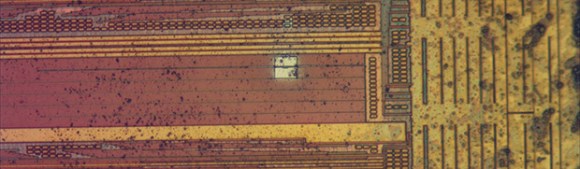
They used focused ion beam (FIB) etching, where a high-speed jet of matter is generated and blasted at a hair to etch the comic. Think of it kind of like a super focused laser beam. Check out the original microscopic imagery of it over on their GitHub.

The cool thing is they really just did this for fun — it’s purpose is to advertise the EHSM conference in Hamburg. The Exceptionally Hard(ware) & Soft(ware) Meeting is a massive gathering of the opensource and DIY hacking world. If you happen to live in Europe we’d recommend checking it out — just take a look at their conference talks they have lined up! The Maker Movement Meets Patent Law, Optics & Photonics with Lego Bricks, the Basics of Quantum Cryptograhy, the Principles of Mass Spectrometry… the list goes on!

Continue reading “World’s Smallest Comic Etched Onto A Human Hair”

Editing Circuits With Focused Ion Beams

CPLD

[Andrew] has been busy running a class on hardware reverse engineering this semester, and figured a great end for the class would be something extraordinarily challenging and amazingly powerful. To that end, he’s editing CPLDs in circuit, drilling down to metal layers of a CPLD and probing the signals inside. It’s the ground work for reverse engineering just about every piece of silicon ever made, and a great look into what major research labs and three-letter agencies can actually do.

The chip [Andrew] chose was a Xilinx XC2C32A, a cheap but still modern CPLD. The first step to probing the signals was decapsulating the chip from its plastic prison and finding some interesting signals on the die. After working out a reasonable functional diagram for the chip, he decided to burrow into one of the lines on the ZIA, the bus between the macrocells, GPIO pins, and function blocks.

Actually probing one of these signals first involved milling through 900 nm of silicon nitride to get to a metal layer and one of the signal lines. This hole was then filled with platinum and a large 20 μm square was laid down for a probe needle. It took a few tries, but [Andrew] was able to write a simple ‘blink a LED’ code for the chip and view the s square wave from this test point. not much, but that’s the first step to reverse engineering the crypto on a custom ASIC, reading some undocumented configuration bits, and basically doing anything you want with silicon.

This isn’t the sort of thing anyone could ever do in their home lab. It’s much more than just having an electron microscope on hand; [Andrew] easily used a few million dollars worth of tools to probe the insides of this chip. Still, it’s a very cool look into what the big boys can do with the right equipment.