The Keychain 6809

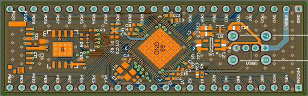
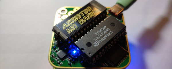
When you think of tiny microcontroller boards, you probably think of a modern surface mount processor. Not [Andreas Jakob]. His 5×5 cm keychain computer rocks a 6809 CPU at a blistering 1 MHz or, if you prefer, a 6309 that runs at 5 MHz. The RAM — all 32K — is in a SMD package to make it fit, but the board also sports a 27C256 EPROM which means that chip and the CPU take up most of the PCB.

As you might expect, there’s not much else on the board. It doesn’t hurt, too, that the PCB is a 6-layer board. The board features a USB C port for power and data, but we didn’t see the USB interface chip on the schematic until we opened it in Easy EDA using the button that says “open in editor.” The schematic says it is sheet 1 or 1, but there are actually two additional “tabs” you can only see in the editor with the apparently missing pieces.

Continue reading “The Keychain 6809”

Thinking About Creating A Raspberry Pi Replacement?

If you’ve ever wanted to try your hand at creating a Raspberry Pi-like board for yourself, you should check out [Jay Carlson’s] review of 10 different Linux-capable SoCs. Back in the 1960s, a computer was multiple refrigerator-sized boxes with thousands of interconnections and building one from scratch was only a dream for most people. Then ICs came and put all the most important parts in a little relatively inexpensive IC package and homebrew computing became much more accessible. Systems on Chip (SoC) has carried that even further, making it easier than ever to create entire systems, like the Pi and its many competitors.

Only a few years ago, making an SoC was still a big project because the vendors often didn’t want to release documentation to the public. In addition, most of the parts use ball grid array (BGA) packaging. BGA parts can be hard to work with, and require a multilayer PC board. Sure, you can’t plug these into a typical solderless breadboard. But working with these relatively large BGAs isn’t that hard and multilayer boards are now comparatively cheap. [Jay] reports that he got cheap PCBs and used a hot plate to build each board, and has some sage advice on how to do it.

Continue reading “Thinking About Creating A Raspberry Pi Replacement?”

A Automated Optical Inspection machine, inspecting the USB Armory board

Meet The Machines That Build Complex PCBs

You can etch a simple PCB at home with a few chemicals and some patience. However, once you get to multilayer boards, you’re going to want to pay someone to do the dirty work.

The folks behind the USB Armory project visited the factories that build their 6 layer PCB and assemble their final product. Then they posted a full walkthrough of the machines used in the manufacturing process.

The boards start out as layers of copper laminates. Each one is etched by applying a film, using a laser to print the design from a Gerber file, and etching away the unwanted copper in a solution. Then the copper and fibreglass prepreg sandwich is bonded together with epoxy and a big press.

Bonded boards then get drilled for vias, run through plating and solder mask processes and finally plated using an Electroless Nickel Immersion Gold (ENIG) process to give them that shiny gold finish. These completed boards are shipped off to another company, where a pick and place followed by reflow soldering mounts all the components to the board. An X-Ray is used to verify that the BGA parts are soldered correctly.

The walkthrough gives a detailed explanation of the process. It shows us the machines that create products we rely on daily, but never get to see.