Some readers out there probably have nostalgic feelings for their first 386 based PC, the beeps and hisses of the modem, and the classic sound of a floppy drive’s stepper motor. Perhaps that turbo button that we could never quite figure out.
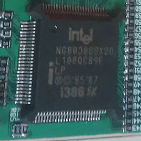
If you want the power of a 386 processor today, you’re in luck: [Pierre Surply] has developed a modern development board for the 80386SX CPU. This board is based on a 386 processor that comes in a LQFP package for “easy” soldering, and an Altera Cyclone IV FPGA.
To allow the CPU to run, the FPGA emulates the chipset you would usually find on a PC motherboard. The FPGA acts as both a bus controller and a memory controller for the CPU. On the board, there’s an SRAM chip and internal memory on the FPGA, which can be accessed through the 386’s bus access protocol.
The FPGA also provides debugging features. A supervisor application running on the FPGA gives debugging functionality via a FTDI USB to UART chip. This lets you control operation of the CPU from a PC for debugging purposes. The FPGA’s memory can be programmed through a JTAG interface.
The project is very well documented, and is a great read if you’re wondering how your old 386 actually worked. It can even be hand soldered, so the adventurous can grab the design files and give it a go. The francophones reading can also watch the talk in the video below.


