Streamline Your SMD Assembly Process With 3D-Printed Jigs

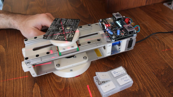
Your brand-new PCBs just showed up, and this time you even remembered to order a stencil. You lay the stencil on one of the boards, hold it down with one hand, and use the other to wipe some solder paste across…. and the stencil shifts, making a mess and smearing paste across the board. Wash, rinse (with some IPA, of course), repeat, and hope it’ll work better on the next try.

openscad window
A PCB jig generated by OpenSCAD

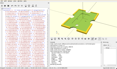
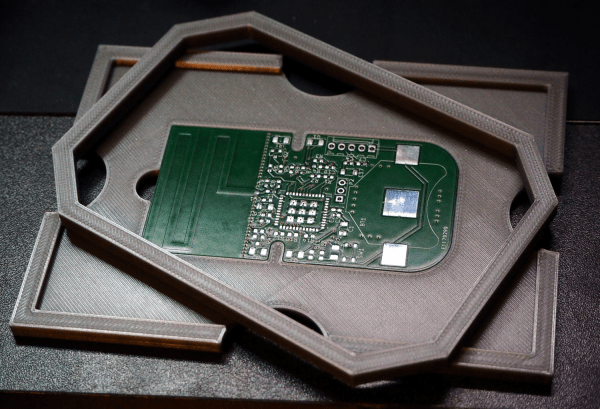
Maybe it’s time to try Stencilframer, a 3D-printable jig generator created by [Igor]. This incredibly useful tool takes either a set of gerbers or a KiCad PCB file and generates 3D models of a jig and a frame to securely hold the board and associated stencil. The tool itself is a Python script that uses OpenSCAD for all 3D geometry generation. From there, it’s a simple matter to throw the jig and frame models on a 3D printer and voilà!– perfectly-aligned stencils, every time.

This is a seriously brilliant script. Anyone whose gone through the frustration of trying to align a stencil by hand should be jumping at the opportunity to try this out on their next build. It could even be paired with an Open Reflow hot plate for a fully open-source PCB assembly workflow.

Continue reading “Streamline Your SMD Assembly Process With 3D-Printed Jigs”

PnPAssist: A “Smart” Build Platform For Manual PCB Assembly

Open source pick and place machines have come a long way in the past years, but are not necessarily worth the setup time and machine cost if you are only building a few PCBs at a time. [Nuri Erginer] found himself in this situation regularly, so he created PnPAssist, a “smart” build platform to speed up manual PCB assembly. Video after the break.

The PnP assist consists of a small circular platform that can automatically translate and rotate to place the current footprint in the middle of the platform, right in the center of your microscope’s view, and a laser crosshair. The entire device can also rotate freely on its base to avoid contorting your arm to match the footprint orientation. Just export the PnP file from your favorite PCB design software, load it on a micro SD card, plug it into the PnPAssist, and start assembling. The relevant component information is displayed on a small OLED display right on the machine. [Nuri] has also created a component organizing tray that will indicate the correct compartment with an RGB LED.

Below the build platform, a 3D printed gear is in contact with a pair of parallel lead screws driven by stepper motors. The relative motion of the lead screws allows the platform to rotate, translate, or both. This arrangement also means the machine is a lot more compact than a conventional XY-table and can be packed away when not in use. The base is held firmly in place on the workbench with a set of suction cups or screws. Power is provided through the fixed base using a slip-ring, so there are no cables to twist up as you spin the machine around. Continue reading “PnPAssist: A “Smart” Build Platform For Manual PCB Assembly”

Slim RGB Matrix Puts LEDs Inside The PCB

Sometimes all that’s required to build something interesting is to put the same old pieces together differently. [Sayantan Pal] did this for the humble RGB LED matrix, creating an extra-thin version by recessing WS2812b NeoPixel LEDs inside a PCB.

The popular WS2812B is 1.6 mm in height, which happens to be the most commonly used PCB thickness. Using EasyEDA, [Sayantan] designed a 8×8 matrix with modified WS2812B footprints. A slightly undersized cutout was added to create a friction-fit for the LEDs, and the pads were moved to the back side of the panel just outside the cutout, and their assignment were flipped. The PCB is assembled face down, and all the pads are soldered by hand. Unfortunately this creates rather large solder bridges which slightly increases the overall thickness of the panel, and is probably also unsuitable for production with conventional pick-and-place assembly.

We’ve seen some similar methods with PCB assemblies that use layered PCBs. Manufacturers are starting to even embed components inside multilayer PCBs.

Parallel Pis For Production Programming; Cutting Minutes And Dollars Off Of Assembly

Assembly lines for electronics products are complicated beasts, often composed of many custom tools and fixtures. Typically a microcontroller must be programmed with firmware, and the circuit board tested before assembly into the enclosure, followed by functional testing afterwards before putting it in a box. These test platforms can be very expensive, easily into the tens of thousands of dollars. Instead, this project uses a set of 12 Raspberry Pi Zero Ws in parallel to program, test, and configure up to 12 units at once before moving on to the next stage in assembly.

Continue reading “Parallel Pis For Production Programming; Cutting Minutes And Dollars Off Of Assembly”

The Components Are INSIDE The Circuit Board

Through-hole assembly means bending leads on components and putting the leads through holes in the circuit board, then soldering them in place, and trimming the wires. That took up too much space and assembly time and labor, so the next step was surface mount, in which components are placed on top of the circuit board and then solder paste melts and solders the parts together. This made assembly much faster and cheaper and smaller.

Now we have embedded components, where in order to save even more, the components are embedded inside the circuit board itself. While this is not yet a technology that is available (or probably even desirable) for the Hackaday community, reading about it made my “holy cow!” hairs tingle, so here’s more on a new technology that has recently reached an availability level that more and more companies are finding acceptable, and a bit on some usable design techniques for saving space and components.

Continue reading “The Components Are INSIDE The Circuit Board”

Product Development And Avoiding Stock Problems

You’ve spent months developing your product, your Kickstarter just finished successfully, and now you’re ready to order all the parts. Unfortunately, your main component, an ATmega328P, is out of stock everywhere with a manufacturer lead time of 16 weeks. Now what?

When manufacturing things in large volumes, acquiring enough stock at the right time can be tricky. There can be seasonal shortages with companies trying to get products manufactured and available for Christmas. There can be natural disasters like floods of hard drive factories, or politically-related availability problems like tantalum for capacitors, or maybe new markets open up that increase demand or a new product sucks up all the available supply. The result is all the same; you have a harder time getting what you need. Fortunately, there are some ways to avoid this problem, or at least mitigate it.

Continue reading “Product Development And Avoiding Stock Problems”

One Person’s Experience Of Having PCB Assembly Done In China

Those of us who have our PCBs manufactured by Chinese PCB fab houses will be used to seeing tempting offers to also assemble our completed boards. Send the Gerbers as normal, but also send a BoM, and for an extra slice of cash you can receive fully assembled PCBs instead of just bare boards. It sounds alluring, but leaves a few questions for those without the experience. How much will it cost, what will the quality be like, and will my boards work? [Alexander Lang] had a limited run of ten small pressure sensor boards to make, and since his board house had started an assembly service,  decided to take the plunge and opt for full assembly.

His first step was to assemble his BoM and send it with the Gerbers. He is at pains to stress that the BoM is key to the whole project, and getting it right with the correct packages and more than one source for each component is critical. The board house first charged him £32.05 ($41.76) to make his PCBs and stencil, and assess his BoM for a build quote. A few days passed, and then he had a quote for assembly, £61.41 ($80). He placed the order, the board house processed it and made the boards, and in due course his working PCB modules arrived.

This might sound at this point like an unexciting saga, but its very smoothness is the key to what makes it interesting. Those of us who have wondered about the risks involved in taking up such a service need to hear stories like this one as surely as we do stories of failure, because without them we’re flying blind. Whether £93.46 ($121.76) for ten small boards represents good enough value is another matter, but if surface-mount soldering is not your thing you might be interested to follow [Alexander]’s example. After all, it wasn’t so long ago that getting a cheap PCB made in China was a similar leap of faith.