Two lamp versions side by side - one desk lamp and one spotlight lamp, both turned on and shining

A Tale Of Two LÄMPs

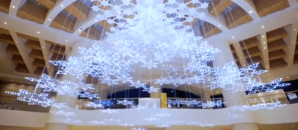
Building with LEDs is a hacker pastime like no other – what’s more, if you keep playing with LED tech out there, you’re bound to build something elegant and noteworthy. For today’s fix of beautiful LED devices, take a look at the two LÄMP creations of [Jana Marie], both LED projects building upon one another. It’s not just your regular RGB LEDs – she adds a healthy mix of white and yellow LEDs, making for colors way more natural-looking and pleasant to the eye!

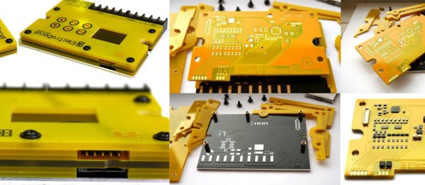
The first one is the LAEMP-Panel, a two-PCB sandwich, combining into a spot light you can use for any purpose where some extra LED would really shine – be it photography, accent, or mood lighting. All of these LEDs are individually controlled and from the SK6812 family, half of them YYW and half RGB variation. As for the base board, the controller is an ESP32, paired to an E75 ZigBee module – this spot light is built to be part of your home’s ZigBee network. If you look at the base board’s KiCad files, you will also notice six-pin headers on five edges – and they’re there for a reason.

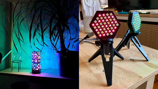
The sister project to this one, the LAEMP-Prism, is a remarkable hexagonal lamp built upon the LAEMP-Panel’s PCB base, but in a desk-friendly form-factor. Six extra side panels with a generous amount of circular cutouts give you a total of 291 LEDs, mix of yellow, white and RGB as before – we got to say, from the pictures we found, it looks like a gorgeous thing to have in your house!

Such is a story of building a spotlight and a desk lamp, both using the same hardware base to accomplish quite different purposes. As is [Jana-Marie]’s tradition, these two lamps are fully open-source, complete with instructions on assembling them – everything is ready for you if you’d like to build one of your own, whichever version it may be! When it comes to lamp-building projects that excel at looks, one can’t forget the two other lamps we’ve seen a few years ago – one built with fiber optics, and another in the shape of the Moon.

SIM Card Connectors And White PCBs Make Huge LED Snowflakes Happen

[Mike Harrison] talked about designing and building a huge scale LED lighting installation in which PCBs were used as both electrical and mechanical elements, and presented at Electromagnetic Field 2016. The project involved 84,000 RGBW LEDs, 14,000 microcontrollers and 25,000 PCBs. It had some different problems to solve compared to small jobs, but [Mike] shared techniques that could be equally applied to smaller scale projects or applications. He goes into detail on designing for manufacture and assembly, sourcing the parts, and building the units on-site.

The installation itself was a snowflake display for a high-end shopping mall in Hong Kong in the 2015 Christmas season. [Mike] wanted a small number of modular boards that could be connected together on-site to make up the right shapes. In an effort to minimize the kinds of manufacturing and parts needed, he ended up using modular white PCBs as structural elements as well as electrical. With the exception of some minor hardware like steel wire supports, no part of the huge snowflakes required anything outside of usual PCB manufacturing processes to make. The fewer suppliers, the fewer potential problems. [Mike] goes into design detail at 6:28 in the video.

For the connections between the boards, he ended up using SIM card connectors intended for cell phones. Some testing led to choosing a connector that matched up well with the thickness of a 1.6mm PCB used as a spacer. About 28,000 of them were used, and for a while in 2015 it was very hard to get a hold of that particular part, because they had cleaned everyone out! Continue reading “SIM Card Connectors And White PCBs Make Huge LED Snowflakes Happen”

Custom Case Made Entirely Out Of PCBs

So you’ve finished your project. You’ve got a wonderful circuit, a beautiful PCB, and everything works perfectly. You’re done right? Well, maybe not. Sure, a bare PCB might be fine for a dev board, but what if you have a LCD to mount, a knob that needs turning, and buttons that need pressing. Yeah, that potentiometer hanging off the board by a few wires isn’t so pretty, is it? So it’s time for a case. Yuck. We all hate modifying cases.

[Electrodacus] came up with a clever solution in the form of stacking PCBs to form a case. In his project, he actually has the circuitry spread across 3 PCBs, and uses surface mount connectors to connect them in a stack. Along the edges are specifically shaped PCBs to complete the enclosure. This technique could be used with only one PCB containing all the circuitry, and the others acting as the case sides and top.

In this solar battery management project, the base layer has most of the power circuitry. This layer uses an aluminum metal core PCB for heat dissipation. The center layer is home for the micro controller and supporting components. And the top layer is the “front panel” with capacitive touch buttons and a cut out for a LCD. The top layer silk screen contains the logo, button markings, and the pin out of all the connectors.

If you hate drilling and filling cases (as much as we do), this technique might be right for your next project.

[via EEVBlog Forums]