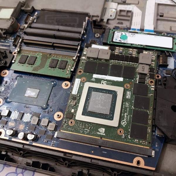
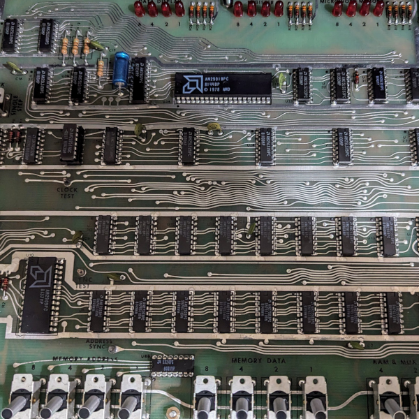
The surest way to reverse engineer a circuit is to look at all the components, all the traces between these components, and clone the entire thing. Take a look at a PCB some time, and you’ll quickly see a problem with this plan: there’s soldermask hiding all the traces, vias are underneath components, and replicating a board from a single example isn’t exactly easy. That’s alright, because [Joe Grand] is here to tell you how to deconstruct PCBs one layer at a time.
Most of this work was originally presented at DEFCON last August, but yesterday [Joe] put up a series of YouTube videos demonstrating different techniques for removing soldermask, delayering multi-layer boards, and using non-destructive imaging to examine internal layers.
If you’re dealing with a two-layer board, the most you’ll have to do is remove the soldermask. This can be done with techniques ranging from a fiberglass scratch brush, to laser ablation, to a dremel flapwheel. By far the most impressive and effective ways to take the solder mask off of PCBs is the way the pros do it: chemically. A bath in Magnastrip 500 or Ristoff C-8 results in perfectly stripped boards and a room full of noxious chemicals. It makes sense; this is what PCB houses use when they need to remove solder mask during the fabrication process.
Removing a solder mask will get you the layout of a two-layer board, but if you’re looking at deconstructing multi-layer boards, you’ll have to delaminate the entire board stack to get a look at the interior copper layers. By far the most impressive way of doing this is with a machine that can only be described as gently violent, but passive, imaging techniques such as X-rays, CT scanners and other sufficiently advanced technology will also do the trick. Acoustic microscopy, or Acoustic Micro Imaging, was, however, unsuccessful. It does look cool, though.
Thanks [Morris] for the tip.


