Chemistry And Lasers Turn Any Plastic Surface Into A PCB

On the face of it, PCB production seems to pretty much have been reduced to practice. Hobbyists have been etching their own boards forever, and the custom PCB fabrication market is rich with vendors whose capabilities span the gamut from dead simple one-side through-hole boards to the finest pitch multilayer SMD boards imaginable.

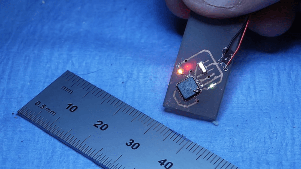
So why on Earth would we need yet another way to make PCBs? Because as [Ben Krasnow] points out, the ability to turn almost any plastic surface into a PCB can be really handy, and is not necessarily something the fab houses handle right now. The video below shows how [Ben] came up with his method, which went down a non-obvious path that was part chemistry experiment, part materials science. The basic idea is to use electroless copper plating, a method of depositing copper onto a substrate without using electrolysis.

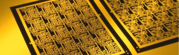
This allows non-conductive substrates — [Ben] used small parts printed with a Formlabs SLA printer — to be plated with enough copper to form solderable traces. The chemistry involved in this is not trivial; there are catalysts and surfactants and saturated solutions of copper sulfate to manage. And even once he dialed that in, he had to figure out how to make traces and vias with a laser cutter. It was eventually successful, but it took a lot of work. Check out the video below to see how he got there, and where he plans to go next.

You’ve got to hand it to [Ben]; when he decides to explore something, he goes all in. We appreciate his dedication, whether he’s using candles to explore magnetohydrodynamics or making plasma with a high-speed jet of water.

Continue reading “Chemistry And Lasers Turn Any Plastic Surface Into A PCB”

The Components Are INSIDE The Circuit Board

Through-hole assembly means bending leads on components and putting the leads through holes in the circuit board, then soldering them in place, and trimming the wires. That took up too much space and assembly time and labor, so the next step was surface mount, in which components are placed on top of the circuit board and then solder paste melts and solders the parts together. This made assembly much faster and cheaper and smaller.

Now we have embedded components, where in order to save even more, the components are embedded inside the circuit board itself. While this is not yet a technology that is available (or probably even desirable) for the Hackaday community, reading about it made my “holy cow!” hairs tingle, so here’s more on a new technology that has recently reached an availability level that more and more companies are finding acceptable, and a bit on some usable design techniques for saving space and components.

Continue reading “The Components Are INSIDE The Circuit Board”

How Commercial Printed Circuit Boards Are Made

Most of us who have dabbled a little in electronics will have made our own printed circuit boards at some point. We’ll have rubbed on sticky transfers, laser-printed onto acetate, covered our clothing with ferric chloride stains, and applied ourselves to the many complex and tricky processes involved. And after all that, there’s a chance we’ll have ended up with boards that were over or under-etched, and had faults. For many the arrival of affordable online small-run professional PCB production from those mostly-overseas suppliers has been a step-change to our electronic construction abilities.

[Fran Blanche] used to make her own boards for her Frantone effects pedals, but as she admits it was a process that could at times be tedious. With increased production she had to move to using a board house, and for her that means a very high-quality local operation rather than one on the other side of the world. In the video below the break she takes us through each step of the PCB production process as it’s done by the professionals with a human input rather than by robots or ferric-stained dilettantes.

Though it’s twenty minutes or so long it’s an extremely interesting watch, as while we’re all used to casually specifying the parameters of the different layers and holes in our CAD packages we may not have seen how they translate to the real-world processes that deliver our finished boards. Some operations are very different from those you’d do at home, for example the holes are drilled as a first step rather than at the end because as you might imagine the through-plating process needs a hole to plate. The etching is a negative process rather than a positive one, because it serves to expose the tracks for the plating process before etching, and the plating becomes the etch resist.

If you’re used to packages from far afield containing your prototype PCBs landing on your doorstep as if by magic, take a look. It’s as well to know a little more detail about how they were made.

Continue reading “How Commercial Printed Circuit Boards Are Made”