Fixing NRF24L01+ Modules Without Going (Too) Insane

Good old nRF24L01+ wireless modules are inexpensive and effective. Well, they are as long as they work correctly, anyway. The devices themselves are mature and well-understood, but that doesn’t mean bad batches from suppliers can’t cause hair-pulling problems straight from the factory.

[nekromant] recently got a whole batch of units that simply refused to perform as they should, but not because they were counterfeits. The problem was that the antenna and PCB design had been “optimized” by the supplier to the point where the devices simply couldn’t work properly. Fortunately, [nekromant] leveraged an understanding of the problem into a way to fix them without going insane in the process. The test setup is shown in the image above, and the process is explained below. Continue reading “Fixing NRF24L01+ Modules Without Going (Too) Insane”

Chip Decapping The Easy Way

Chip decapping videos are a staple of the hacking world, and few things compare to the beauty of a silicon die stripped of its protective epoxy and photographed through a good microscope. But the process of actually opening that black resin treasure chest seems elusive, requiring as it does a witch’s brew of solvents and acids.

Or does it? As [Curious Marc] documents in the video below, a little heat and some finesse are all it takes, at least for some chips. The method is demonstrated by [Antoine Bercovici], a paleobotanist who sidelines as a collector of old chips. After removing chips from a PCB — he harvested these chips from an old PlayStation — he uses hot air to soften the epoxy, and then flexes the chip with a couple of pairs of pliers. It’s a bit brutal, but in most of the Sony chips he tried for the video, the epoxy broke cleanly over the die and formed a cleavage plane that allowed the die to be slipped out cleanly. The process is not unlike revealing fossils in sedimentary rocks, a process that he’s familiar with from his day job.

He does warn that certain manufacturers, like Motorola and National, use resins that tend to stick to the die more. It’s also clear that a hairdryer doesn’t deliver enough heat; when they switched to a hot air rework station, the success rate went way up.

The simplicity of this method should open the decapping hobby up to more people. Whether you just want to take pretty pictures or if reverse engineering is on your mind, put the white fuming nitric acid down and grab the heat gun instead.

Continue reading “Chip Decapping The Easy Way”

Tidy Board Rework Uses Flex PCBs, No Wires

PCB rework for the purpose of fixing unfortunate design problems tends to involve certain things: thin wires (probably blue) to taped or glued down components, and maybe some areas of scraped-off soldermask. What are not usually involved are flexible PCBs, but [Paul Bryson] shows us exactly how flex PCBs can be used to pull off tricky rework tasks.

It all started when [Paul] had a run of expensive PCBs with a repeated error; a design mistake that occurred in several places in the board. Fixing with a bunch of flying wires leading to some glued-on components just wasn’t his idea of tidy. A more attractive fix would be to make a small PCB that could be soldered in place of several of the ICs on the board, but this idea had a few problems: the space available into which to cram a fix wasn’t always the same, and the footprints of the ICs to be replaced were too small to accommodate a PCB with castellated mounting holes as pads anyway.

It’s about then that he got a visit from the Good Idea Fairy, recalling that fab houses have recently offered “flex” PCBs at a reasonable cost. By mounting the replacement parts on a flex PCB, the board-level connection could reside on the other end of an extension. Solder one end directly to the board, and the whole flexible thing could be bent around or under on a case-by-case basis, and secured in whatever way made sense. Soldering the pads of the flex board to the pads on the PCB was a bit tricky, but easy enough to pull off reliably with a bit of practice. A bonus was that the flex PCB is transparent, so solder bridges are easy to spot. He even mocked up a solution for QFP packages that allows easy pin access.

Flex PCBs being available to hobbyists and individuals brings out fresh ideas and new twists on old ones, which is why we held a Flexible PCB Design Contest earlier this year. Repairs were definitely represented as applications, but not to the extent that [Paul] has shown. Nice work!

Fixing Fake FTDIs

If you know where to go on the Internet, you can pick up an FTDI USB to Serial adapter for one dollar and sixty-seven cents, with free shipping worldwide. The chip on this board is an FTDI FT232RL, and costs about two dollars in quantity. This means the chips on the cheap adapters are counterfeit. While you can buy a USB to serial adapter with a legitimate chip, [Syonyk] found a cheaper solution: buy the counterfeit adapters, a few genuine chips, and rework the PCB. It’s brilliant, and an excellent display of desoldering prowess.

Why is [Syonyk] replacing non-genuine chips with the real FTDI? The best reason is FTDIgate Mk. 1, where the official FTDI driver for Windows detected non-genuine chips and set the USB PID to zero. This bricked a whole bunch of devices, and was generally regarded as a bad move. FTDIgate Mk. 2 was a variation on a theme where the FTDI driver would inject garbage data into a circuit if a non-genuine part was found. This could also brick devices. Notwithstanding driver issues, the best reason for swapping out fake chips for real ones is the performance at higher bit rates; [Syonyk] is doing work at 3 Mbps, and the fake chips just don’t work that fast.

To replace the counterfeit chip, [Syonyk] covered the pins in a nice big glob of solder, carefully heated both sides of the chip, and slid the offending chip off when everything was molten. A bit of solder braid, and the board was ready for the genuine chip.

With the new chip, the cheap USB to serial adapter board works perfectly, although anyone attempting to duplicate these efforts might want to look into replacing the USB mini port with a USB micro port.

Halogen Lamp Abused For Desoldering

[Moony] thought that it was unconscionable that IR soldering stations sell for a few hundred Euros. After all, they’re nothing more than a glorified halogen lightbulb with a fancy IR-pass filter on them. Professional versions use 100 W 12 V DC bulbs, though, and that’s a lot of current. [Moony] tried with a plain-old 100 W halogen lightbulb. Perhaps unsurprisingly, it worked just fine. Holding the reflector-backed halogen spotlight bulb close to circuit boards allows one to pull BGAs and other ornery chips off after a few minutes. Voila.

[Moony] reasons that the IR filter is a waste anyway, since the luminous efficiency of halogen lights is so low: around 3.5%. And that means 96.5% heat! But there’s still a lot of light streaming out into a very small area, so if you’re going to look at the board as you de-solder, you’re really going to need a pair of welding goggles. Without, you’ll have a very hard time seeing your work at best, and might actually do long-term damage to your retinas.

So the next time you’re feeling jealous of those rework factory workers with their fancy IR soldering stations, head on down to the hardware store, pick up a gooseneck lamp, a 100 W halogen spotlight, and some welding goggles. And maybe a fire brick. You really don’t want your desk going up in flames.

We love make-do hacks, but we love doing it right, too. Just watch [Bil Herd] extol the virtues of a real IR desoldering station. And then giggle as you do the same thing with a few-dollar halogen bulb.

Continue reading “Halogen Lamp Abused For Desoldering”

Creating New Nintendo 3DS Hardware

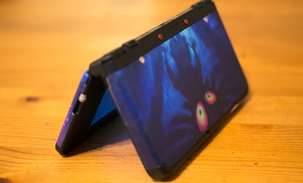
For the last five years or so, Nintendo has been selling the 3DS, the latest in a long line of handheld consoles. Around two years ago, Nintendo announced the New Nintendo 3DS, with a faster processor and a few other refinements. The new 3DS comes in two sizes: normal and XL. You can buy the XL version anywhere in the world, but Nintendo fans in North America cannot buy the normal version.

[Stephen] didn’t want the jumbo-sized New 3DS XL, both because it’s too large for his pockets, and because there are no fancy cases for the XL. His solution? Creating a US non-XL 3DS with god-like soldering skills.

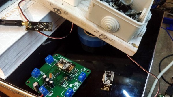
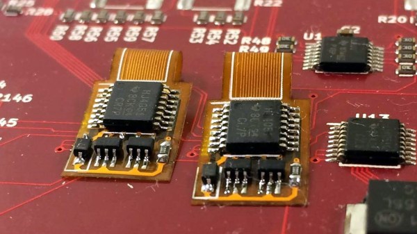
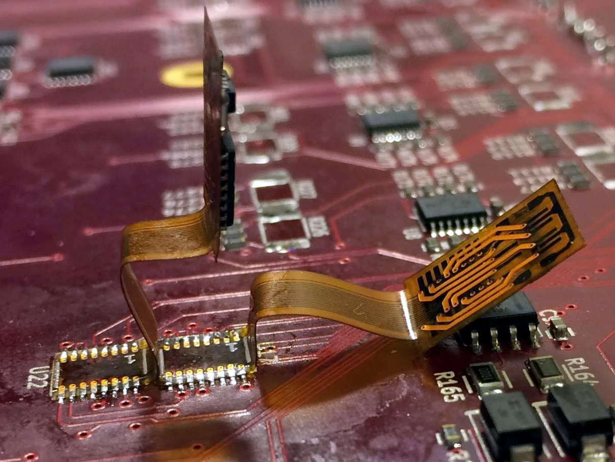
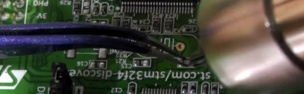
In manufacturing the XL and non-XL versions of the 3DS, Nintendo didn’t change much on the PCBs. Sure, the enclosure is different, but electronically there are really only two changes: the eMMC storage and the Nintendo processor. 3DS are region-locked, so simply swapping out the boards from a normal 3DS to an XL 3DS wouldn’t work; [Stephen] would also like to play US games on his modded console. That leaves only one option: desoldering two chips from a US XL and placing them on the board from a Japanese 3DS.

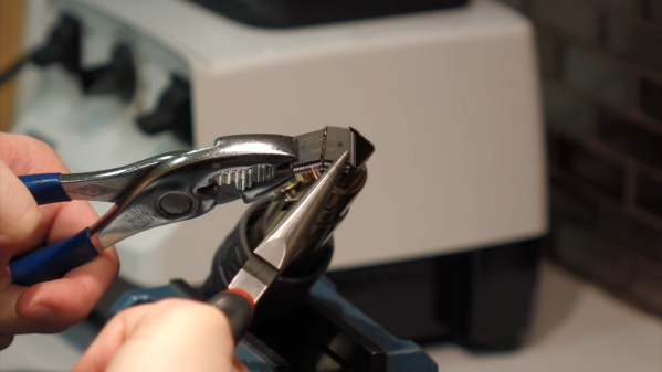
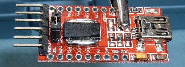
With a board preheater and heat gun, [Stephen] was able to desolder the eMMC chip off both boards. Of course this meant the BGA balls were completely destroyed in the process, which means reballing the package with solder bits only 0.3mm in diameter. With the US eMMC transplanted to the Japanese board, [Stephen] ended up with an error message that suggested the processor was reading the memory. Progress, at least.

[Stephen] then moved on to the processor. This was a nightmare of a 512 pin BGA package, with 512 pins that needed a tiny dot of solder placed on them. Here, sanity gave way and [Stephen] called up a local board and assembly house. They agreed to solder the chip onto the board and do an x-ray inspection. With the professional rework done, [Stephen] assembled his new US non-XL 3DS, and everything worked. It’s the only one in the world, and given the effort required to make these mods, we’re expecting it to remain the only one for a very long time.

Swapping Dev Board Crystals To Suit Your Needs

Microcontroller Dev Boards have the main hardware choices already made for you so you can jump right into the prototyping by adding peripherals and writing code. Some of the time they have everything you need, other times you can find your own workarounds, but did you ever try just swapping out components to suit? [Andy Brown] documented his process of transplanting the clock crystal on an STM32F4 Discovery board.

Even if you don’t need to do this for yourself, the rework process he documented in the clip after the break is fun to watch. He starts by cleaning the through-hole joints of the crystal oscillator with isopropyl alcohol and then applies some flux paste to each. From there the rest is all hot air. The crystal nearly falls out due to gravity but at the end he needs to pluck it out with his fingers. We’re happy to see others using this “method” as we always feel like it’s a kludge when we do it. Next he grabs the load caps with a pair of tweezers after the briefest of time under the heat.

We’d like to have a little bit of insight on the parts he replaces and we’re hoping there are a few crystal oscillator experts who can leave a comment below. [Andy] calculates a pair of 30pf load caps for this crystal. We understand the math but he mentions a common value for board and uC input capacitance:

assuming the commonly quoted CP + CI = 6pF

So we asked and [Andy] was kind enough to share his background on the topic:

It’s a general “rule of thumb” for FR4 that the stray capacitance due to the traces on the board and the input (lead) capacitance of the the MCU is in in the range of 4-8pF. I’m used to quoting the two separately (CP,CI) but if you look around you’ll see that most people will combine the two and call it just “CP” and quote a value somewhere between 4 and 8pF. It’s all very “finger in the air” and for general purpose MCU clocks you can get away picking the mid-value and be done with it.

That leaves just one other question; the original discovery board had an in-line resistor on one of the crystal traces which he replaces with a zero ohm jumper. Is it common to include a resistor and what is the purpose for it?

Continue reading “Swapping Dev Board Crystals To Suit Your Needs”