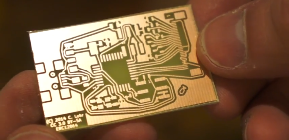
If you’re going to learn something, it only makes sense to learn from a master. [CNLohr] is known around these parts for his fablous PCBs, and he’s finally started to document his entire fabrication process.
[CNLohr] is using a photoetch process, where a mask is created with a laser printer on overhead transparencies. He covers the copper clad boards with a Riston photosensitive mask—available here, and they accept Bitcoin—sent through a laminator, and exposed with the laser printed mask and a UV grow bulb. After the mask has developed, [CNLohr] drops his boards into a ferric chloride bath that eats away the unexposed copper. He then removes the photomask with acetone and cuts the boards with a pair of aircraft snips, and they’re ready to be soldered up with components.
Yes, home PCB etching tutorials are pretty much a solved problem, but [CNLohr]’s work speaks for itself. He’s also the guy who made a microcontroller/Linux/Minecraft thing on a glass microscope slide. Learning from a guy with these skills means you’re learning from one of the best.
Video below, and there’s also a video going over the design of a PCB using KiCAD (!) and TopoR (!!!) available here.