Circuit Love With Multicolor Solder Masks

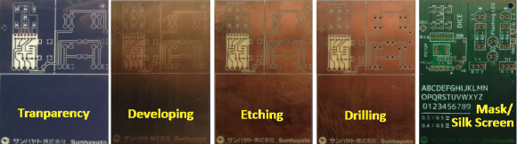
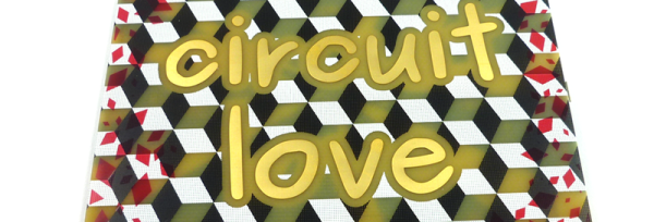
The cheapest PCBs – and therefore most common – are green solder mask with white silkscreen. It works, but it’s also incredibly boring. This is the way things were done up until a few years ago with the explosion of board houses trying to compete for your Yuan, and now getting a red, yellow, black, blue, green, and even OSH purple is possible. This doesn’t mean multiple solder masks aren’t possible, as [Saar] demonstrates with his demonstration of multicolor solder masks and circuit love.

We’ve seen a lot of [Saar]’s designs, including a mixing desk, a cordwood puzzle, and an engineer’s emergency business card, but so far his artistic pieces have been decidedly monochromatic. For this build, [Saar] teamed up with Eurocircuits to create a board that exploits their capabilities.

Althought Eurocircuits has PCB PIXture, a tool for putting graphics on PCBs, [Saar] made this with his own tool, PCBmodE.  The design of both the red and yellow variants are abstract, and only meant to be a demonstration of what can be done with multicolor solder mask. It looks great with five backlit LEDs, and with an acrylic top and bottom, makes a great coaster or art piece.

We like [Saar’s] work so much that we put his Cordwood puzzle in the Hackaday Store.

DIY Circuit Boards Look Professional

Professional Looking DIY PCB Boards

Making PCBs at home is a great means to get your prototype up and running without having to wait weeks for a professionally made board. Regardless if these prototype boards are milled or etched, they are easily identified as ‘home brew’ due to their ‘unfinished’ appearance. [HomeDIY&Stuff] has put together a little how-to on the process for making DIY PCBs look a little closer to a professionally manufactured board.

The process starts out with designing the board in a PCB program. There are a lot of these programs available. Eagle is a popular choice and has a free version available. Once the layout it finalized, the design is printed out on a transparent sheet of plastic. A blank copper-clad PCB board that already has a UV sensitive coating applied are available for purchase and is what is used in this example. The transparency is placed over the PCB blank and then exposed to UV light. The coating on the PCB cures where ever the UV light passes through the open areas of the transparency.

Once the transparency is removed, there is a noticeable difference in coating color where it has cured. This board is now placed in a developer solution that removes the un-cured UV sensitive coating. A Ferric Chloride acid bath then etches away at the now-exposed copper. The cured coating from the previous step protects the copper at the trace locations during the etch process. The result is a board with copper where you want it and none where you don’t. If the board has any through-hole components, this would be the time to drill those holes.

Up to this point the process has been pretty standard for homemade PCBs and the next part is certainly the most interesting but, unfortunately, is also the worst documented step; the solder mask and silk screening. It appears that two silk screens are produced, one for the solder mask and one for the silk screen. The artwork for making the silk screens can be output from the PCB design software. There is no mention of the solder mask material used but oil-based silk screen ink is specified. Although the details are lacking, the photos show that it works pretty well. If you have had any experience with silk screening DIY PCBs, let us know in the comments.

One-Off Kapton Solder Masks

soldermask

With the proliferation of desktop routers, and a number of easy methods to create PCBs at home, there’s no reason anyone should ever have to buy a pre-made breakout board ever again. The traditional techniques only give you a copper layer, however, and if you want a somewhat more durable PCB, you’ll have figure out some way to create a solder mask on your homebrew PCBs. [Chris] figured Kapton tape would make a reasonable soldermask, and documented the process of creating one with a laser cutter over on the Projects site.

The solder mask itself is cut from a piece of Kapton tape, something that should be found in any reasonably well-stocked tinkerer’s toolbox. The software for [Chris]’ laser cutter, a Universal Laser Systems model, already has a setting for mylar film that came in handy for the Kapton tape,

Of course, getting the correct shapes and dimensions for the laser to cut required a bit of fooling around in Eagle and Corel Draw. The area the laser should cut was taken from the tCream and tStop layers in Eagle with a 1 mil pullback from the edges of the pads. This was exported to an .EPS file, opened in Corel Draw, and turned into a line art drawing for the laser cutter.

The result is a fast and easy solder mask that should be very durable. While it’s probably not as durable as the UV curing paints used in real PCBs, Kapton will be more than sufficient for a few prototypes before spinning a real board.

Polyurethane Protecting PCBs

PCB

What you see above is a home-made PCB. No, this isn’t an example of a terrible toner transfer job, but rather evidence of the ravages of time. This board is seven years old, and the corrosion and broken traces show it. Luckily, [George] already has seven years of environmental data for a cheap DIY soldermask.

Seven years ago, [George] took a piece of copper clad board, masked half of it off, and sprayed it with fast drying polyurethane. After drying, he put it on a shelf in his garage. The results were fairly surprising – the uncovered portion is covered in verdigris, while the coated half is still shiny and new.

[George] took this a bit further and experimented with other spray can coverings. He found Testors spray enable worked just like the polyurethane, burning off when the heat of a soldering iron was applied, and also passed for a professional PCB.

Put A Solder Mask On Those Homebrew PCBs

While making your own PCBs at home is one of the best marks of a competent builder, if you want to give your project a more professional vibe, you’re going to need to do better than bare copper traces on a piece of fiberglass. To help out his fellow makers, [Chris] sent in his Instructable on creating a solder mask for homemade circuit boards using a minimal amount of tools and materials easily sourced from the Internet.

[Chris]’ soldermasks are made from UV curing paints he found on eBay. Of course the traditional green paint is available, along with paints very similar to the Sparkfun red or Arduino blue soldermasks.

After brushing the soldermask paint onto his home-etched circuit board, [Chris] printed out the solder mask onto a piece of transparency film using a laser printer. This mask is vitally important if you ever plan to solder your board; by covering the pads you wish to solder, the paint won’t cure and can later be removed.

[Chris] cured his soldermask by leaving it in the sun for a half hour. After the paint was dry, he removed the excess paint covering the pads with a little bit of turpentine and some elbow grease.

While [Chris]’ paint had somewhat of an ugly matte finish, the soldermask does its job, protecting the PCB traces while leaving the pads uncovered and ready to solder.

Kapton Tape Aids In Drag Soldering Surface Mount Parts

Drag soldering works exactly as its name implies, by dragging a bead of solder across fine-pitch pins you can quickly solder an entire row. The method relies on clean joints, so liquid solder flux is often used to make sure there is good flow. But if you’re drag soldering on boards that you’ve etched yourself the solder can sometimes run down the trace, rather than staying where you want it. Professionally manufactured boards don’t have this problem since they have solder mask covering the copper that doesn’t need soldering. [Ahmad Tabbouch] has a method that uses Kapton tape to act as a temporary solder mask on diy boards.

The process involves several steps. First, three strips are place horizontally across the board, leaving just a portion of the upper and lower pads exposed. Those pads are then tinned with solder, and a light touch with an X-acto knife is then used to score the tape covering the vertical rows of pads. Once the waste as been removed, two more strips are added and those rows are tinned. From there the chip is placed and soldered as we’ve seen before; first tacked in place, then fluxed, and finally drag soldered to complete the connections. This achieves a crisp and clean connection, presumably without the need to clean up your solder mess with solder wick.

Kapton tape resists heat, making it perfect for this process. We’ve also seen it used on hot beds for 3D printers, and as a smoothing surface for sliding mechanisms.

[via Dangerous Prototypes]