Typically, when we want to build something with a DC motor, we might grab a bunch of AAs, or a single lithium cell at the very least. Electric toothbrushes often run on more humble power sources, like a single NiMH battery. They’re designed to get useful motion out of just 1.2V, and [Marian Hryntsiv] has taken a look at what makes them tick.
The article focuses on an electric toothbrush built around the Low Voltage GreenPAK™ SLG47513 chip. It’s designed to work at voltages from just 1 to 1.65 V. To make the most of the limited power available, the toothbrush stays in sleep mode most of the time when it’s not working in oral health.
[Marian] steps through the various parts of the circuit, and also explains the unique functionality baked into the brush. Of particular interest are the timer routines that guide the user through brushing each section of the mouth in turn, before a notification that tells them that 2 minutes of brushing time has elapsed. There’s also a useful explanation of the inductive charging method used.
Electric toothbrushes may be mundane home items today, but they’re an example of a product that has largely already been optimized to the nth degree. Until laser-based plaque removal or enamel regeneration technology gets off the ground, this is as good as it gets. We can dream, though!
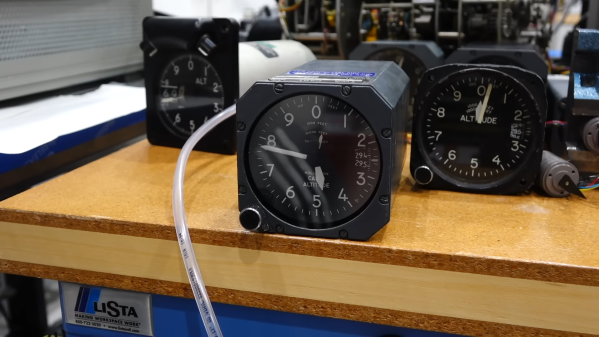
There’s a strange synchronicity in the projects we see here at Hackaday, where different people come up with strikingly similar stuff at nearly the same time. We’re not sure why this is, but it’s easily observable, with this vintage altimeter teardown and repair by our good friend [CuriousMarc] as the latest example.
The altimeter that [Marc] dissects in the video below was made by Kollsman, which is what prompted us to recall this recent project that turned a jet engine tachometer into a CPU utilization gauge. That instrument was also manufactured by Kollsman, but was electrically driven. [Marc]’s project required an all-mechanical altimeter, so he ordered a couple from eBay.
Unfortunately, thanks to rough handling in transit they arrived in less than working condition, necessitating the look inside. For which we’re thankful, of course, because the guts of these aneroid altimeters are quite impressive. The mechanism is all mechanical, with parts that look like something [Click Spring] would make for a fine timepiece. [Marc]’s inspection revealed the problem: a broken pivot screw keeping the expansion and contraction of the aneroid diaphragms from transmitting force to the gear train that moves the needles. The repair was a little improvisational, with 0.5-mm steel balls used to stand in for the borked piece. It may not be flight ready, but it worked well enough to get the instrument back in action.
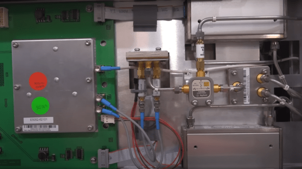
[Shahriar] of The Signal Path is back with another fascinating video teardown and analysis for your viewing pleasure. (Embedded below.) This time the target is an Agilent E5052A 7 GHz signal Source/Analyser which is an expensive piece of kit not many of us are fortunate enough to have on the bench. This particular unit is reported as faulty, with a signal power measurement that is completely off-the-rails wrong, which leads one to not trust anything the instrument reports.
After digging into the service manual of the related E5052B unit, [Shahriar] notes that the phase noise measurement part of the instrument is totally separate from the power measurement, only connected via some internal resistive power splitters, and this simplifies debugging a lot. But first, a short segue into that first measurement subsystem, because it’s really neat.
Cross-correlating time-gated FFT (TG-FFT) subsystem at the top, dodgy power detector at the bottom
A traditional swept-mode instrument works by mixing the input signal with a locally-sourced low-noise oscillator, which when low-pass filtered, is fed into a power meter or digitizer. This simply put, down-converts the signal to something easy to measure. It then presents power or noise as a function of the local oscillator (LO) frequency, giving us the spectral view we require. All good, but this scheme has a big flaw. The noise of the LO is essentially added to that of the signal, producing a spectral noise floor below which signals cannot be resolved.
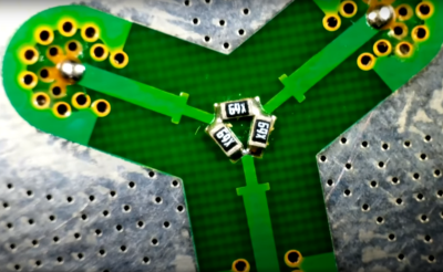
The E5052 instrument uses a cunning cross-correlation technique enabling it to measure phase noise levels below that of its own internal signal source. The instrument houses an Oven-Compensated Crystal Oscillator (OCXO) for high stability, in fact, two from two different vendors, one for each LO, and mounted perpendicular to each other. The technique splits the input signal in half with a power splitter, then feeds both halves into identical (apart from the LOs) down-converters, the outputs of which are fed into a DSP via a pair of ADCs. Having identical input signals, but different LOs (with different phase noise spectra) turns the two signals from a correlated pair to an uncorrelated pair, with the effects of chassis vibration and gravity effects also rolled in.
The DSP subtracts the uncorrelated signal from the correlated signal, therefore removing the effect of the individual LO’s effect on the phase noise spectrum. This clever technique results in a phase noise spectrum below that of the LOs themselves, and a good representation of the input signal being measured.
This is what a DC-7GHz resistive power divider looks like. Notice the inductive matching section before each resistor branch.
Handily for [Shahriar] this complex subsystem is totally separate from the dodgy power measurement. This second system is much simpler, being fed with another copy of the input signal, via the main resistive power splitter. This second feed is then split again with a custom power divider, which upon visual inspection of the input SMA connector was clearly defective. It should not wobble. The root cause of the issue was a cold solder joint of a single SMA footprint, which worked loose over time. A little reflow and reassembly and the unit was fit for recalibration, and back into service.
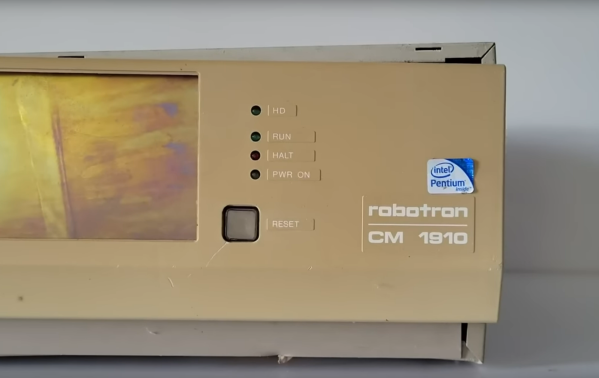
There are plenty of bizarre computers around from the 70s through the 90s before the world somewhat standardized around various duopolies of hardware vendors and operating systems. Commodore, Atari, and even Apple had some bizarre machines from this era but for our money, the most unusual systems come out of the Eastern Bloc. We’ve featured plenty of these before, and the latest is a Robotron CM1910 which comes to us from [Chernobyl Family] via YouTube.
Built in East Germany behind the wall, the Robotron factories had easier access to Soviet than western parts, but the latter were also available when necessary. Hence it’s built on an Intel 8086 processor, which seems common enough for the era, but after opening the case some non-standard construction becomes apparent.
The first is a densely-packed array of circuit boards and wiring, far beyond what a western PC might have included in this time. This also partially explains its massive 25 kg weight. It does include a hard drive, two floppy disk drives, a large dedicated graphics card, and a modem which all contribute as well. The overall design philosophy of the machine was a headscratcher too, which would have involved near-complete dismantling of the machine to access or repair some of the parts, as well as some hidden peripheral and drive controllers in questionable locations.
From the looks of it, we doubt this computer will see any uptime anytime soon, although they did at least restore the keyboard. With all of the chips accessible on PCBs, it might be possible to get this machine up and running again although it would take a massive effort thanks to its non-standard design and construction, and might also require help from builds like this to replace or emulate some of the hardware.
Modern insulin pumps are self-contained devices that attach to a user’s skin via an adhesive patch, and are responsible for administering insulin as needed. Curious as to what was inside, [Ido Roseman] tore down an Omnipod Dash and took some pictures showing what was inside.
A single motor handles inserting the cannula into the skin, retracting the insertion needle, and administering insulin.
These devices do quite a few things. In addition to holding a reservoir of insulin, they automatically insert a small cannula (thin tube) through the skin after being attached, communicate wirelessly with a control system, and pump insulin through the cannula as needed. All in a sealed and waterproof device. They are also essentially disposable, so [Ido] was curious about what kind of engineering went into such a thing.
The teardown stops short of identifying exactly how all the mechanisms inside work, but [Ido] was able to learn a few interesting things. For example, all of the mechanical functions — inserting the cannula with the help of a needle (and retracting the needle afterwards) and pumping insulin — are all accomplished by one motor and some clever mechanical engineering.
The electronics consist of a PCB with an NXP EX2105F 32-bit Arm7 microcontroller, a second chip that is likely responsible for the wireless communications, three captive LR44 button cells, and hardly a passive component in sight.
The software and communications side of an insulin pump like this one has had its RF communications reverse-engineered with the help of an SDR, a task that took a lot more work than one might expect. Be sure to follow that link if you’re interested in what it can take to get to the bottom of mystery 433 MHz communications on a device that isn’t interested in sharing.
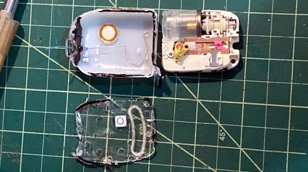
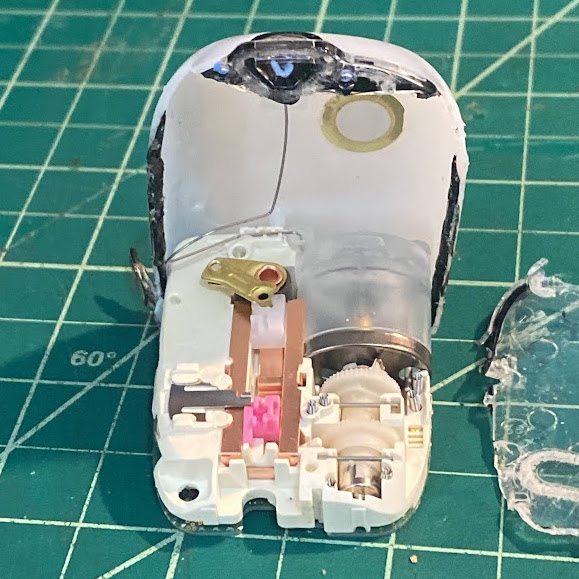
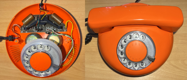
The 20th century saw everything from telephones to computers become mainstream. Many of these devices were beautifully designed in the mid-century period, something that’s hard to say about a lot of today’s cheaper technology. [John Graham-Cumming] has shown us one exquisite example, with his teardown of a simple Czech telephone.
The model in question is a DS3600 telephone built by Tesla Stropkov in the early 1980s. Despite this, it’s a design that looks like it hails more from the 1960s based on its smooth curves and rounded features. It’s a rotary dial phone, though a push-button version was also produced.
Inside the phone is a simple single-sided PCB clearly marked out with a tidy silkscreen. The ringer and a few capacitors make up the bulk of the circuitry inside the base, along with the rotary dial. The handset itself plays host to most of the other componentry, including the mystery “WNB 068 hybrid circuit” which [John] couldn’t positively identify.
It’s great to get a look inside vintage hardware and see how things were done in yesteryear. It’s particularly funny to think about how simple telephones used to be in contrast to today.
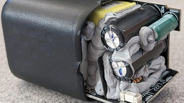
Every so often, a new technology comes along that offers a broad range of benefits over what we already have. Just as lithium-ion batteries have made nickel-cadmium cells boring and old hat, gallium nitride semiconductors are making silicon parts look unimpressive by comparison. [Brian Dipert] looked at what this means in a practical sense by tearing down a GaN phone charger.
The charger in question is a 30 watt USB-C charger produced by Voltme. It cost [Brian] just $10, as prices of GaN hardware have come down significantly as economies of scale have kicked in. The charger measures just 1.2×1.3×1.2 inches, and weighs only 1.5 ounces. That compact size is thanks to GaN semiconductors, which are able to run cooler at higher power levels than their silicon forebearers.
Cracking into the charger required levering open the case. The back panel came off with some work, revealing the mains terminals, which deliver AC power to the PCB inside via the case holding them in contact. Interestingly, the entire circuit inside is filled with an adhesive thermal goop, which helps pass heat from the hottest components to the charger’s case. [Brian] is able to guide us through the circuit, and he identified many of the major components. However, some of the markings on chips were beyond his research skills, and he asks any knowing readers to contribute their own information.
It’s interesting to see just what makes the high-powered compact chargers of today tick. Plus, it’s a hallmark of progress that what was once considered a wonder material can now be had in a $10 commodity phone charger from Amazon. How times change!