DIY Smartwatch Based On ESP8266 Needs Classification

Building your own smartwatch is a fun challenge for the DIY hobbyist. You need to downsize your electronics, work with SMD components, etch your own PCBs and eventually squeeze it all into a cool enclosure. [Igor] has built his own ESP8266-based smartwatch, and even though he calls it a wrist display – we think the result totally sells as a smartwatch.

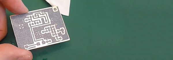
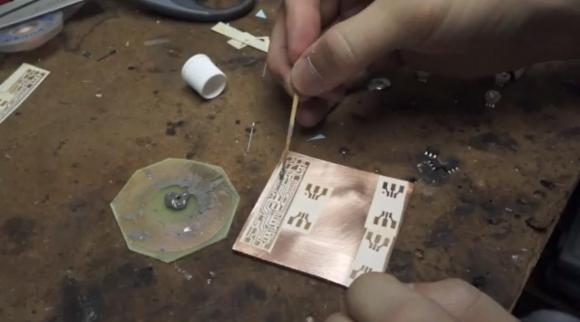
His design is based on a PCB for a wireless display notifier he designed earlier this year. The design uses the ESP-12E module and features an OLED display, LEDs, tactile switches and an FT232R USB/UART interface. Our beloved TP4056 charging regulator takes care of the Lithium-ion cell and a voltage divider lets the ESP8266’s ADC read back the battery voltage. [Igor] makes his own PCBs using the toner transfer method, and he’s getting impressive results from his hacked laminator.

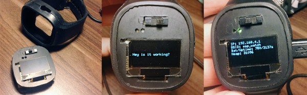
Together with a hand-made plastic front, everything fits perfectly into the rubber enclosure from a Jelly Watch. A few bits of Lua later, the watch happily connects to a WiFi network and displays its IP configuration. Why wouldn’t this be a watch? Well, it lacks the mandatory RTC, although that’s easy to make up for by polling an NTP time server once in a while. How would our readers classify this well-done DIY build? Let us know in the comments!

Even Easier Toner Transfer PCBs

One of the most popular methods of homebrew PCB fabrication is the toner transfer process. Compared to UV-sensitive films and CNC mills, the toner transfer process is fantastically simple and only requires a laser printer. Being simple doesn’t mean it’s easy, though, and successful toner transfer depends on melting the toner to transfer it from a piece of paper to a copper clad board.

This is heatless toner transfer for PCB fabrication. Instead of using a clothes iron or laminator to transfer toner from a paper to board, [simpletronic] is doing it chemically using acetone and alcohol.

Acetone usually dissolves laser printer toner, and while this is useful for transferring a PCB from paper to board, it alone is insufficient. By using a mixture of eight parts alcohol to three parts acetone, [simpletronic] can make the toner on a piece of paper stick, but not enough to dissolve the toner or make it blur.

From there, it’s a simple matter of putting a piece of paper down on copper clad board. After waiting a few minutes, the paper peels off revealing perfectly transferred board art. All the usual etching techniques can be used to remove copper and fabricate a PCB.

This is an entirely novel method of PCB fabrication, but it’s not exactly original. A few days ago, we saw a very similar method of transferring laser printed graphics to cloth, wood, and metal. While these are probably independent discoveries, it is great evidence there are still new techniques and new ways of doing things left to be discovered.

Thanks [fridgefire] for the tip.

Toner Transfer And Packing Tape

The toner transfer process of producing PCBs has evolved tremendously over the last few years. It started out by printing PCB layouts onto magazines with a laser printer, then some clever people figured out that glossy inkjet photo paper would work just as well. Now there’s a new substrate for you – packing tape – and it seems to work pretty well.

[David] was designing a cheap board for a robot kit for a workshop and needed 100 tiny PCBs. They were simple boards, and perfectly suited for home PCB manufacturing. He started off by printing directly onto glossy magazine paper, but this wasn’t an ideal solution. During one run, some of the toner landed on the packaging tape he was using to secure the boards. A bit of serendipity came into play and [David] discovered packaging tape is usable in the toner transfer process.

The technique is simple enough: put some packaging tape on a piece of paper, print a board layout (reversed!) on a laser printer, and go through the usual clothes iron/laminator/etching process. [David] is actually using a hair straightener for transferring the toner over to the copper clad board – interesting, and in a pinch you can use the same tool for reflowing SMD components.

Upgrading A Laminator For Toner Transfer PCBs

If you need a circuit board now, you’re probably looking at a toner transfer process; all you need to make a PCB is a copper clad board, a laser printer, some special paper, and the usual etching chemicals. The quality of these boards is highly dependant on the quality of transferring toner to the copper, and getting the process right is as much an art as it is a science. A clothes iron is the easy way of transferring the toner to the board, but if you’re looking for repeatability, you’ll probably want a laminator.

Laminators, too, also vary in quality. The king of toner transfer laminators is the Apache AL13P. With four heated rollers and a steel chassis, it’s enough to do some serious heating. [mosaicmerc] came up with an amazing mod for his Apache laminator that takes all the guesswork out of the settings, and does it all in one pass for maximum repeatability and PCB quality.

The Apache laminator in question is a beast of a machine that drives four rollers with a synchronous motor and also has a ‘reverse’ button that sends the laminations out the front end of the printer. Stock, a toner transfer PCB would require dozens of passes through the Apache, but [merc]’s mod takes care of everything for you.

The addition that makes this possible is a small board with a PIC12 microcontroller. This microcontroller connects the motor driver board and the display interface together, triggering the reverse button to move the board 5/8″ forward and 1/2″ back, giving the laminator an effective speed reduction of 12:1. This method also has the bonus of not tampering with the motor or control circuitry, and allows for multiple passes in the same run.

With this modification, the Apache AL13P becomes the perfect solution to transferring toner to a piece of copper, with the ability to transfer 10mil traces on 1oz copper. The board also offers some other features like thermal sensor failure shutdown and a cool-down mode that overrides the heater. If you’re looking for an easy way to step up your toner transfer PCBs, you can’t do much better than this mod.

Toner Transfer PCBs, Double Sided, With Color Silkscreen

Silk

Making a few PCBs with the toner transfer method is a well-known technique in the hacker and maker circles. Double-sided PCBs are a little rarer, but still use the same process as their single-sided cousins. [Necromancer] is taking things up a notch and doing something we’ve never seen before – double-sided PCBs made at home, with color silkscreens, all make with a laser printer.

For laying down an etch mask, [Necro] is using a Samsung ML-2167 laser printer and the usual toner transfer process; print out the board art and laminate it to some copper board.

The soldermasks use a similar process that’s head-slappingly similar and produces great results: once the board is etched, he prints out the solder mask layer of his board, laminates it, and peels off the paper. It’s so simple the only thing we’re left wondering is why no one thought of it before.

Apart from the potential alignment issues for multiple layers, the only thing missing from this fabrication technique is the ability to do plated through holes. Still, with a laser printer, a laminator, and a little bit of ferric or copper chloride you too can make some very nice boards at home.

Perfect PCBs With An Inkjet Printer

Instead of mucking about fabbing PCBs with the toner transfer method, or making masks for photosensitive boards, the holy grail of at-home circuit board manufacturing is a direct inkjet-to-etch method. [Don] isn’t quite there yet, but his method of producing circuit boards at home is one of the easiest we’ve ever seen.

[Don]’s boards begin by taking the output from Eagle and printing them with an Epson Artisan 50 inkjet printer. By sticking a piece of cardstock in the printer before the copper board, he’s able to precisely align the traces and pads onto the copper board.

When the board comes out of the printer, it’s only covered in ink. While some specialty inks are enough of an etch resist, [Don] comes up with a clever way to make sure acid doesn’t eat away copper in the needed places – he simply dusts on toner from a copier or laser printer, blows off the excess, and bakes the entire board in a toaster oven.

The result, seen above, are perfect traces on a circuit board without the need for ironing sheets of photo paper onto copper boards.

As far as the, “why didn’t someone think of this sooner” ideas go, this one is at the top. [Don] says the method should work  on sheets of aluminum for printing solder paste masks. Impressive work, and now the only thing left to do is getting two-layer boards down pat. For more direct to copper printing check out the hacks we’ve covered in years past.

Continue reading “Perfect PCBs With An Inkjet Printer”

DIY Heatsinking PCBs

pcb heatsink

We have covered many do it yourself PCBs before, but this video guide adds an easy way to sink heat from high power devices, which we think you might find handy.

It is a very simple process that [CNLohr] uses to keep his small RGB LED projects from overheating. It starts by using a readily available silicone thermal sheet as the substrate by applying it to copper foil. He then applies a toner-transfer circuit pattern to the copper by running the pair through a modified laminator a few times. He makes note that you have to apply the plastic backing side of the silicone sheet to the copper foil to prevent the laminator from chewing it up.

After the typical ferric chloride etching process is complete, he then uses 220 grit sandpaper to remove the toner pattern. Often steel wool is used, but because of the sensitive nature of the silicone, sandpaper works better to avoid peeling up traces.

We have featured [CNLohr] before, as he does some top-notch tutorials in his workshop — which makes for both a fascinating and distracting backdrop for the videos. This one is a bit long (~20 minutes), but is very thorough and goes through the entire process from start to finish. Check it out after the break.

Continue reading “DIY Heatsinking PCBs”