Usually, repairing a device entails replacing a defective IC with a new one. But if you’ve got young eyes and haven’t had caffeine in a week, you can also repair a defective chip package rather than replace it.
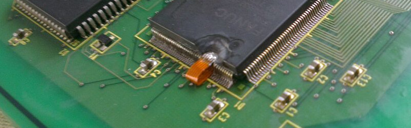
There’s no description of the incident that resulted in the pins of the QFP chip being ablated, but it looks like a physical insult like a tool dropped on the pins. [rasminoj]’s repair consisted of carefully grinding away the epoxy cap to expose the internal traces leading away from the die and soldering a flexible cable with the same pitch between the die and the PCB pads.
This isn’t just about [rasminoj]’s next-level soldering skills, although we’ll admit you’ve got to be pretty handy with a Hakko to get the results shown here. What we’re impressed with is the wherewithal to attempt a repair that requires digging into the chip casing in the first place. Most service techs would order a new board, or at best solder in a new chip. But given that the chip sports a Fanuc logo, our bet is that it’s a custom chip that would be unreasonably expensive to replace, if it’s even still in production. Where there’s a skill, there’s a way.
Need more die-level repairs? Check out this iPhone CPU repair, or this repair on a laser-decapped chip.
[via r/electronics]


Now those are soldering skills to DIE for.
Groan.
What could be used as a reasonably suitable encapsulant ( let´s say, in an equipment that is not that costly ) ?
Also, about the tooling ? Dremel with some microscopic bits ?
Yeah, Dremel in like that. I am on the look for some 2nd-hand dentist tools to experiment with. I think some of those drill bits could be of the right size. Also, don´t remember where I saw it, but I mean to experiment with a laser burner for vaporizing some part of the encapsulation.
Hot glue. Lots of hot glue lol
Spilled super caps
Been there, done that.
More than once, I lifted a QFP pin, to isolate it from the PCB track, and broke it, so I had to solder a small wire directly to the remains of the pin.
Not rocket science.
I think many of us have been there, but soldering to a remnant nub is a bit easier than grinding down the package to expose and solder to the leadframe
Amen, brother!
I’ve done this to re-purpose repairable spill damaged purpose-built E-POS equipment as test-rigs.
As long as it is only some low power leaded chip that had their leads electro-etched away and it wasn’t caused by a 12v rail eating away at a 1.2v logic pin due to said spillage.
Some such PCBs are quite robust… especially if the pads have all been gold plated first before soldering as the gold plating slows the corrosion on the board side to a salvageable state albeit with the copper under the delaminated gold coatings being exposed/tarnished.
Opening the lead frame to expose a salvageable amount has saved things ranging from RS232 level shifters, LPC to IO/legacy controllers and all sorts. Also quicker to just throw a milling bit down in a chuck and expose the pads than wrecking a $400 mainboard attempting to replace the fragile-state component on fragile pads.
Thanks for posting this. Saw it on the same subreddit a few days ago. Based on the comments there and here, I get the impression that this sort of repair is simple and common for a small subset of electronics folks and completely foreign and amazing for the rest of us — in other words, exactly the kind of technique that should be shared with a wider audience!
IMO, it’s one of those things that you figure out how to do when you get to the level of experience needed to do it.
I dunno about the fancy tools. I’ll bet you could make this work with a file, a utility knife, a bunch of flux, flat flex, and a decent temp-controlled station. In other words, anyone with $100ish to spend and a decent bit of patience.
Thing is… I’ve done it this way before… Also that chloro-something “plastic weld” stuff makes a good resin softener for making such a task like this easier. Work decided the stuff was a bit too potent (towards humans) and for health and safety reasons blacklisted it from getting ordered.
Well, some botched jobs can be just discarded, on the basis of the amateur destroyed it, or the prices for repairing it can be adjusted accordingly.
But it is interesting to divulge the possibilities of this kind of repair so that people just do not dismiss something as unrepairable and just scrap the board. We have many cases here where people just want to throw away something because “It can´t be repaired” or “it is damaged and impossible to repair “, and I almost have to force them to show / bring me the boards to look at. And these are boards with SOIC chips, When I say I will just replace the chip, they go “That can be done ? “. Sadly, common people are getting too distant of the possibilities or realities of physical things….
I already blame them for a lot of things, even global warming, so one more thing is easy to add to the list. :)
Ages since I had to do this, guess I wasn’t desperate enough, or it wasn’t valuable enough. It was on an SOJ DRAM, on a graphics card.
Not a die.
:o/
I wonder if you could add leads to a package that can output signals based on some internal component of the die. Might need to have some strange coupling they leads to a driver circuit, but that could be interesting…
That 3M tape that conducts in the Z axis is excellent for this sort of thing.
As long as you can get one with the necessary resolution (?) between parallel tracks
small strip
https://www.amazon.com/Adafruit-Z-Axis-Conductive-Tape-9703/dp/B00SK8L4R2
small roll
https://www.amazon.com/Z-Axis-Electrically-Conductive-Double-Sided/dp/B00K3377EG
could it be a $500 i/o modbus board?
respect!
Wow, speechless. A new goal to strive for some day. Impressive! Maybe a CNC mill printer soldering kit can aid with some sort of sensor to detect materials is what I was thinking. By hand… yes, impressive.
Right, still… why not be elaborate? :-|)
I was thinking automated rework station with custom IC repair or even custom IC’s made. OK, the later is overboard. Vapo deposition wouldn’t be so home brew easy with the kit. Maybe as an additional option however?
Well… yeah… I’m more used to setting up machines for tools to be made and not the electronic IC’s. You know better at this kind of task/project.
Excellent work and example. I never even had the thought of performing such a task.
Correct.
I’m at the “wanting to program FPGA’s skill level that has updated firmware well over a dozen times, just ordered a GQ 4×4 and new sockets to solder in for the EPROM and NVRAM on the TDS-520 for future potential maintenance.” Really, studying still for now because I’m scared regarding my de-soldering skills. Though went with echodelta’s bellow idea and a desoldering tool with spring loaded sucker built in that I will modify as I found similar on instructables.
Chips are not as big a deal programming. I was even thinking there must be a way with the Arduino to program the 32 pin DIN chips, though… didn’t pursue reading.
I even confused co-workers at one time when they were like… you want to make specifications for firmware and place in a what???… DQ… and test for in the hardware IQ… isn’t that software and supposed to be in the software validation teams docs???.
Some day… maybe… I will advance to the skill level of making or modifying chips with my hands. I know I can. For now… feasible with automation that I don’t have the time and skills to learn yet. Other projects await.
The repair is really awesome and impressive!
I purchased directly from the MCUmall website. I almost was going to purchase a cheaper ~$40 one, though I had already invested in a GMC-320 Plus from GQ Electronics and thought the product and support were great and I didn’t have to custom build anything because at the time I was on the road.
I was successful in reading and writing to a Dallas DS1245Y chip and haven’t gotten into the TDS-520 EPROM chip yet. Still trying to verify missing resistors and am planning on replacing three capacitors if not more since 16V 85’C are present and I think 105’C would be better if not double the voltage also for the A11 module.
I also was having issues with the plugin manager updating for Notepad ++ for some reason so never got around to the hex editor converter plugin.
Really neat learning compared to an Arduino that isn’t as broad application, or at least COTS as versatile from what I’ve read.
Looking forward to investing in adapters and studying and programming other chips. I think I am going to salvage components and chips from an old Zenith and IBM motherboard. Interesting how the Zenith chips are entirely socketed… of which I may restore… though thinking for a Win95 system trying to build the most modern hardware like a P3 or P4 would be beneficial. I also want to try the custom Win95 kernels for newer mobo’s.
20 years ago, the company I worked for contracted with another firm to repair an IC with a design flaw by rerouting a trace on the IC. This was with 0.6 micron technology; I don’t know how small are the features this sort of work can be done on.
“That’s not the die, it’s the leadframe and you need encapsulant on the repair.”
Glad I wasn’t the only one screaming that at my computer.
@ǝıuuɐ
Yeah, I recently received a range of DIN socket adapters for various chips to be able to read the chips as well as probe connectors though not sure about being able to read and write “in socket” or “in circuit” will work. I assume will have to remove… though I have seen on eBay some old “clothes pin” clip wide jaw pin tip adapters that clamp onto the DIN IC’s pins with plugs for wire leads for in circuit testing. I haven’t seen a clamp square type chip version though.