From the sound of reports in the press, graphene is the miracle material that will cure all the world’s ills. It’ll make batteries better, supercharge solar panels, and revolutionize medicine. While a lot of applications for the carbon monolayer are actually out in the market already, there’s still a long way to go before the stuff is in everything, partly because graphene can be very difficult to make.
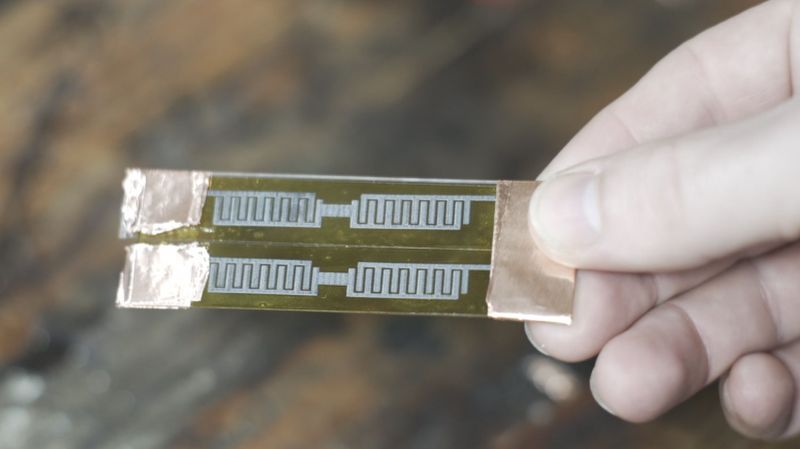
It doesn’t necessarily have to be so hard, though, as [Zachary Tong] shows us with his laser-induced graphene supercapacitors. His production method couldn’t be simpler, and chances are good you’ve got everything you need to replicate the method in your shop right now. All it takes is a 405-nm laser, a 3D-printer or CNC router, and a roll of Kapton tape. As [Zach] explains, the laser energy converts the polyimide film used as the base material of Kapton into a sort of graphene foam. This foam doesn’t have all the usual properties of monolayer graphene, but it has interesting properties of its own, like extremely high surface area and moderate conductivity.
To make his supercaps, [Zach] stuck some Kapton tape to glass slides and etched a pattern into with the laser. His pattern has closely spaced interdigitated electrodes, which when covered with a weak sulfuric acid electrolyte shows remarkably high capacitance. He played with different patterns and configurations, including stacking tape up into layers, and came up with some pretty big capacitors. As a side project, he used the same method to produce a remarkable effective Kapton-tape heating element, which could have tons of applications.
Here’s hoping that [Zach]’s quick and easy graphene method inspires further experimentation. To get you started, check out our deep-dive into Kapton and how not every miracle material lives up to its promise.
Thanks to [Sebastian] for the tip.


Can we get some ballpark values for the kind of capacitance from that? Like the piece in the picture, how many nF is that one?
Heya, video-creator here :) The supercap in the HaD photo (four cells in series) clocked in at 21uF and somewhere around 2.5V. The one in the YT thumbnail (single cell) was 156uF and 0.8V.
Note: I’m not a huge electronics person tbh, and measured voltage with a multimeter. I’ve since learned that might not be very accurate since it discharges the cap a lot faster than I expected… so take the voltage numbers with a grain of salt. The literature says that the single-cell version should be around 1V
If you’re measuring voltage on the device without charging it first, then you’ve built a battery, not a capacitor.
I charged them :) Juiced them on my lab power supply, then checked voltage on multimeter. They just discharge very quickly (likely due to DIY manufacturing issues).
Capacitance readings were taken fully discharged, per the instructions of the meter.
OK. I didn’t catch the charging step in the video.
Yeah that’s totally my fault, I don’t think I said it explicitly in the video. I had some more explanations that I ended up cutting because they were confusing… I think that was a casaulty of the editing process on accident :(
I might do a followup video, with a longer explanation and some corrections / tips I received in the comments (better/alternative ways to test them in particular). Also sorta want to make a big 20V cap or something too :)
Cheers!
To be honest, this is not graphene. It is most likely not even graphitized carbon. Most likely yoi have some amorphous crap over thererl, that you are trying to pass of as graphene. Because the name is flashy.
What you are seong is more a consequence of the geometry you picked, rather than the material.
If you are interested in finding out what you have after butning capton (becaise this is what you are doing), you can send me a piece of it and I can measure raman and xrd for you. If there is anytging that ressembles graphene in it, it will show a very cpear sognature in the spectra.
To be fair, this is how academia labels this material: https://scholar.google.com/scholar?hl=en&as_sdt=0%2C46&q=%22laser+induced+graphene%22&btnG=
If you read the papers, they make it clear this is a foamy mixture of graphene, fullerenes, nano and microtubes, amorphous carbon, etc. But there is strong, repeated evidence that graphene is being generated in both pure monolayer flakes and degenerate 5-7 graphene by raman shift
My test samples behave as the literature suggests (using very similar lasers… papers use everything from excimer up to CO2, the wavelength doesn’t particularly matter for polyimide) so I dont have any reason to believe it’s _not_ laser induced graphene. Not trying to be flashy, honestly.. if the papers called it “laser induced amorphous carbon” I would have used that in the title instead. Just trying to replicate the papers that I’ve read. :)
That said I’d love to get it tested on a Raman! I looked into purchasing one but even “hobbyist” varieties are expensive :) How can I get in touch with you?
Peel and stick ultra thin heating tape? Have you called up SpaceX or NASA? ;) Ought to be plenty of uses for a next thing to weightless heater in space applications.
This makes me wonder. Is the tape emitting long wave Infra Red?
Print a 50 cm by 50 cm panel and power it up.
There’s evidence that this could be painted on substrates more durable than tape.
Building a heating element to dump wind power into is interesting.
156.1nF. Right at the start of the video.
He actually said uF. Impressive
156 uF, actually. Kinda incredible. As in: not credible.
Only 0.8V. Saturated with sulfuric acid. I wonder at what point a “supercap” is actually a battery.
Really neat idea to carbonize Kapton tape like that though. Gotta try it.
Ok, now I feel inclined to view it. Bc looking at the picture, I’d have guessed maybe 150pF would be plausible, for ordinary materials. 150nF would be a bit surprising, but not too exciting. But 150uF, in that? If so, how the heck? I do believe you’re onto something
You can get some bizzare fuel cell effects from carbon. Two pencil leads with bubbles of hydrogen and oxygen sticking to them will generate a voltage, which goes away if you agitate, and persists more than you might expect.
Could be electric double layer busisness, I don’t really understand this stuff, but it acts a lot like a fuel cell.
156.1uF not nF. Its right at the start of the video.
Batteries are a completely different chemical process… Could there be some battery like activity here, maybe – but looks like its probably a cap to me..
If you look at the area/volume of this vs a commercial cap it doesn’t seem quite so shockingly high as this is pretty large (I admit I was surprised it was that high), but its plausible at least, foamed up carbon plates for both sides means a truly massive surface area – sure the bits in the middle of the fingers are not as big a contributor as the edges where its closest approach but its still there doing something – I don’t know how much surface area this foaming created, but compared to a flat sheet of similar dimensions its going to be very much higher, so its logical it can hold a rather substantial charge.
So grain of salt, since I’m not an expert, but my understanding is that these types of supercaps form helmholtz double layers at the interface between graphene and electrolyte. So positive and negative ions in the electrolyte separate to the two electrodes and associate with the oppositely charged graphene surface, which is what allows supercaps to charge/discharge quickly and have a relatively high capacitance due to the large interface with the electrolyte.
Definitely closer to battery chemistry in that it’s ionic in nature, rather than just charge stored across a dielectric. There’s no actual electrochemical reaction going on though, which I _think_ is what differentiates these type of EDLC supercaps from batteries. I think :)
My laser can easily make <50um lines. I wonder how well this process can make tiny wheatstone-bridge strain gauges? They're usually stupid expensive for the legit ones. On the ToDo list it goes…
Definitely! I didn’t mention it, but there is a whole other area of research around LIG using it for different types of sensors. They can act as capacitive sensors, strain/stretch sensors, and I even saw one using it as a microphone diaphragm. :) E.g. here is capacitive and strain: https://www.mdpi.com/1424-8220/19/16/3477#
Acording to wikipedia, the kapton and “space blanket” (heat reflecting foil in first-aid kid) are more or less the same thing. space blanket is thinner and coated with aluminum on one side… Might be interresting to see if that can be converted as well, since it is cheap to get in big squares (rather than tape) and the aluminum might have some interresting properties if used correctly. It might increase conductivity of the electrodes or it might short-circuit the cap :-)
What Wikipedia entry states that?
Not to say that aluminized polyimide doesn’t exist outside the aerospace industry, but the “space blanket” an everyday Joe and the rest of us peons get is aluminized Mylar (PET, polyester). A remarkable material in its own right, but it ain’t Kapton.
I would have definitely made the two sides interleaved along the whole slide, with a single connective strip along each long edge, and the fingers as small as possible. IIRC capacitance is hugely impacted by surface area and distance between electrodes.
What about this foamed conductor on each side of a single strip of polyamide with polyamide as the insulator? Alternately, many layers of tape with each layer lazed on one side and stuck together would allow greater parallel capacitance.
I wish I could play with the hackerspace laser.
Polyimide (PI, Kapton), not polyamide (PA, nylon), but no matter: interposing a dielectric layer as insulator will effectively negate the effort: you’re putting a tiny capacitor (that dielectric) in series with the supercap. You’ve just changed a 1V 150 uF cap into a 1kV, 150 pF cap…
Next step, electroplate or laser sinter the carbon film with different metals to adjust electrical properties. I’m seeing lots of possibilities here.
At the very least, it’s an easy way of making very thin, flexible PCBs or FRCs at home.
This is not graphene. This is some amorphous carbon thing you have there. Probably not even graphitized. This is yet another nice sell of “graphene” that has nothing to do with graphene.
Your results are a result of the geometry you’ve picked, not the material.
If you are interested in figuring out in what is in burnt capton tape (because this is what you have), you can send me a piece of it and i will measure for you. We can figure out the carbon configuration from Raman and XRD.
To quote the video poster:
To be fair, this is how academia labels this material: https://scholar.google.com/scholar?hl=en&as_sdt=0%2C46&q=%22laser+induced+graphene%22&btnG=
If you read the papers, they make it clear this is a foamy mixture of graphene, fullerenes, nano and microtubes, amorphous carbon, etc. But there is strong, repeated evidence that graphene is being generated in both pure monolayer flakes and degenerate 5-7 graphene by raman shift
My test samples behave as the literature suggests (using very similar lasers… papers use everything from excimer up to CO2, the wavelength doesn’t particularly matter for polyimide) so I dont have any reason to believe it’s _not_ laser induced graphene. Not trying to be flashy, honestly.. if the papers called it “laser induced amorphous carbon” I would have used that in the title instead. Just trying to replicate the papers that I’ve read. :)
That said I’d love to get it tested on a Raman! I looked into purchasing one but even “hobbyist” varieties are expensive :) How can I get in touch with you?
It may be a battery – gas battery using trapped oxygen and hydrogen in that carbon structure. Electrolysis one way and fuel cell the other way. Capacity of such batteries is very small, but that isn’t in contradiction with experiment.
Not at 0.8 to 1V it’s not. No gas generation happens below 1.23V in water based electrolytes. That’s exactly why the maximum voltage is so low, to prevent it from electrolysing.
I had a crack at this a few years back with a cheap NeJe laser engraver. The hardest part I found was getting the laser to give a nice even burn without leaving lines in the graphene print. This causes issues with continuity along the print. Also I was limited to a 35mm square print space.
Another production method for my database of homemade electronics components. I wonder if focused sunlight would also work?
“… wonder if focused sunlight would also work?”
The best power density you can get from focused sunlight is around 10 watts per square millimeter.
A cheap 405 nm laser can deliver about 50 kilowatts per square millimeter.
What do you think?
you can melt steel with focused sunlight so yeah suuuuure whatever you say 10W/mm2 /sarcasme off
You’re welcome to do the calculation or measurement yourself, but it’s true.
Your innumeracy and ignorance won’t change the fact, and is no excuse for your attempt at sarcasm.
either your assumptions are faulty, you didn’t explain properly or your just plain wrong. on a sunny day you get about 1000w/m2 meaning if you take a concave mirror or fresnel lens of about 1 m2 even if the focus point is not perfect you will get densities way higher than 10 measly watt
Snow: There’s nothing to explain: it’s basic optics. You could easily do it yourself but clearly didn’t, so let’s walk through it…
Pick a reasonable lens, say an f/2. Let’s make it a nice simple 1m diameter; its focal length will be 2m. The sun is a half degree wide, so (assuming you have a perfect lens) it will form a spot 17 mm in diameter, or 227 square millimeters.
That 1 m diameter lens will have 785 watts hitting it. Assuming it all gets perfectly transmitted, no reflection, no absorption, that delivers 785/227 = 3.45 watts per square millimeter at the focus.
You can do a bit better with a faster lens, even better with some mirror configurations, and even more with some exotic high-index materials. But it’s really tough to get more than 10 watts per square millimeter from focusing sunlight, and thermodynamically impossible to get more than 50. Wishing the sunlight to focus to a smaller point won’t work.
Even the world’s biggest solar furnace — the one at Odeillo, where the Parker Solar Probe was tested — only manages around 7 watts per square millimeter.
ok TBH i didn’t do the math and i see your point but may i point out that the OP question was not specific enough to assume a single optical element you could still use multiple lenses or mirrors to obtain much higher densities. in your original statement you made it sound like 10w/mm2 was an absolute limit which it is not.
could still use multiple lenses or mirrors to obtain much higher densities
No, you can’t. Optics simply doesn’t work that way, and conjecture won’t change that. Study the concept of etendue to learn more.
You’re fundamentally limited by the surface brightness (power density) of the sun: you simply can’t focus its light to be any brighter than the source. That fundamental limit is around 50 watts per square mm, but any real optical system you can build will be limited to much less. Practically, 10 W/mm^2 is about the best you can do in a real system.
If you were to, through the power of wishful thinking, somehow magically concentrate sunlight to higher than the power density at the surface of the sun, you would a) have a focal spot brighter than the sun, and so it would radiate more power than it would receive; b) be in violation of the second law of thermodynamics; c) be rich, because you’ve just built a genuine free energy device.
ok so i guess im missing something why cant you use multiple elements in parallel and overlap the beams? that’s what they did here https://www.youtube.com/watch?v=8tt7RG3UR4c as far as i can tell.
now im thoroughly confused but guess i might be mixing up energy and power again.
a heat pump doesn’t violate thermodynamics even thought the “source” is weaker that the output doesn’t change the total energy in the system why is optic any different?
don’t get it……
never mind i give up.
Melting steel is dramatic, but a bit of a party stunt. It only requires a temperature of 2000K: equivalent to less than one watt per square millimeter. Go ahead: figure it out yourself with the Stefan-Boltzmann equation. It’s easy. Note the albedo or emissivity is not important here — it cancels out, since at equilibrium the absorbed power equals the radiated power.
The “combining beams” is exactly what a lens or mirror does, but there’s a pretty fundamental limit to how much you can concentrate or combine (specifically: 4pi steradians).
Don’t give up. This stuff is just high school physics and common sense. Don’t get distracted by the woo peddlers and youtube eyeball merchants.
What about using sunlight to pump a laser? Technically it should still count.
I think that you didn’t answer the actual question, because you don’t know either having never tried it.
Absolutely correct. You’ll also note I made no claim to. In the Socratic way, it’s intended to make you think about the question.
Once you do the estimate and realize there is a factor of 5000 between the expected power densities of the two sources, it should occur to you that the mechanism of action may be different and the result might not be comparable. To blithely assume it’s going to be similar is naive, and this simple thought exercise will inform you that you should probably at least test the idea.
Except somebody has already used sunlight to drive a CNC based silicon dioxide (sand) fusor. Given that I think that we can safely say that Kapton doesn’t stand a chance. :-) For me the only question is how to do the optics such that the average hacker could replicate it. Any concrete information in that area would help the entire community, but if you’d prefer to just mastabate can I suggest you find a quiet corner to do it rather than in this public space? :-))
Clearly not getting it, but no matter. No point trying to explain any further.
*plonk*
BTW: You misspelled “mathdebate.”
Very interesting, thank you all.
Would probably work even better using 2W M140 and 3 element glass lens.
Incidentally small amounts of yellow Kapton tape can be had from old LiPo cells and its extensively used in cheap LED lights specifically the mains variety.
It can typically be unwrapped from itself and stuck onto a glass slide without too much hassle.