[CNLohr]’s Glass PCB Fabrication Process

One of [CNLohr]’s bigger claims to fame is his process for making glass PCBs. They’re pretty much identical to regular, fiberglass-based PCBs, but [CNLohr] is building circuits on microscope slides. We’ve seen him build a glass PCB LED clock and a Linux Minecraft Ethernet thing, but until now, [CNLohr]’s process of building these glass PCBs hasn’t been covered in the depth required to duplicate these projects.

This last weekend, [CNLohr] put together a series of videos on how he turns tiny pieces of glass into functional circuits.

At the highest level of understanding, [CNLohr]’s glass PCBs really aren’t any different from traditional homebrew PCBs made on copper clad board. There’s a substrate, and a film of copper that is etched away to produce traces and circuits. The devil is in the details, and there are a lot of details for this build. Let’s dig deeper.

Continue reading “[CNLohr]’s Glass PCB Fabrication Process”

Glass PCB LED Clock

This clock looks fantastic because of the glass PCB used for the build. This banner image allows you to see all the traces and components, but when it is lifted off of the desk surface the LEDs which make up the 7-segment digits appear to be floating.

The concept isn’t new, but it’s a much larger format than we’ve seen before. When we first looked at [CNLohr’s] glass PCB fabrication he was using microscope slides. This uses a much larger pane of glass but it seems the fabrication still uses copper foil glued to the glass, then toner transfer etched like normal.

Here he’s testing out some 74LV164 chips as constant current drivers. One of the commenters on the Reddit thread is skeptical about using the chip in this way and so are we. But as the video after the break shows, it seems to work (at least for now). [CNLohr] also mentions that the AVR soldered on the display is burnt out which doesn’t help his case. Still, we love the look and can’t wait to see where he goes from here!

Continue reading “Glass PCB LED Clock”

Glass PCBs


Our friend [Jeri] tipped us off about this cool video on youtube where the author makes his own “transparent” PCB’s using some nontraditional materials. One ounce copper foil is found online along with some clear glass microscope slides, from there it is just a matter of cementing the foil onto the glass slides with some thin UV curing glue. Once the 2 parts are mated the entire thing is popped into an eeprom eraser for its intense UV light, then excess is trimmed.

The normal routine of toner transfer is used to copy a circuit pattern onto the copper clad glass and it’s etched in standard ferric chloride. The copper is removed but the UV glue that was holding it is still left, some special care needs be followed as this stuff is pretty weak against even mild solvents, and you do not want your traces peeling up. Next no clean solder paste is applied and parts are soldered down with a heat gun, keeping the glass evenly heated to prevent it from cracking.
This leaves you with a board that looks like frosted glass, and in order to protect the glue while clearing up the frosted effect, some polyurethane is applied which fills in all the little bumps and smoothes the surface bout out to almost 100% clear.
The end application in this video is a touch sensitive board which works fine though the back side of the glass and presents a nice smooth interface for the user. Join us after the break for the video.

Continue reading “Glass PCBs”

RGB Glasses Built From PCBs

Shutter shades were cool once upon a time, but if you really want to stand out, it’s hard to go past aggressively bright LEDs right in the middle of your face. A great way to achieve that is by building a pair of RGB glasses, as [Arnov Sharma] did.

The design intelligently makes use of PCBs to form the entire structure of the glasses. One PCB makes up the left arm of the glasses, carrying an ESP12F microcontroller and the requisite support circuitry. It’s fitted to the front PCB through a slot, and soldered in place. The V+, GND, and DATA connections for the WS2812B LEDs also serve as the mechanical connection. The right arm of the glasses is held on in the same way, being the same as the left arm PCB but simply left unpopulated. A little glue is also used to stiffen up the connection.

It’s a tidy build, and one that can be easily controlled from a smartphone as the ESP12F runs a basic webserver which allows the color of the glasses to be changed. It’s not the first time we’ve seen a flashy pair of LED shades either! Video after the break.

Continue reading “RGB Glasses Built From PCBs”

Faux Silkscreen On A PCB Made With A Laser Cutter

If you’re getting PCBs professionally made, silkscreen usually comes free as part of the package. However, if you’re making your own, the job is on you. [Tony Goacher] makes his own PCBs on a CNC router, so he’s not getting any silkscreening as part of that bargain. But he wondered—could he do something analogous with a laser cutter?

The answer is yes. The silkscreen layer was first exported from DesignSpark, with the file then sent to LightBurn to prep it for laser cutting. The board outline layer was first engraved on to a piece of scrap as an alignment aid. Then, the board was placed in the laser cutter, with the silkscreen scorched directly on to the fiberglass.

The results are encouraging, if imperfect. [Tony] says he ran at “quite fast speed at quite high power.” The markings are all there, but they’re a little melty and difficult to read. He noted at lower speeds and lower power, the results were a bit more readable.

PCBs aren’t really an ideal engraving or laser marking material, but this technique could be servicable for some basic markings on DIY PCBs. We look forward to seeing how [Tony] improves the process in future. Video after the break.
Continue reading “Faux Silkscreen On A PCB Made With A Laser Cutter”

Retrotechtacular: Circuit Potting, And PCBs The Hard Way

There was a time when the very idea of building a complex circuit with the intention of destroying it would have been anathema to any electrical engineer. The work put into designing a circuit, procuring the components, and assembling it, generally with point-to-point wiring and an extravagant amount of manual labor, only to blow it up? Heresy!

But, such are the demands of national defense, and as weapons morphed into “weapon systems” after World War II, the need arose for electronics that were not only cheap enough to blow up but also tough enough to survive the often rough ride before the final bang. The short film below, simply titled Potted and Printed Circuits, details the state of the art in miniaturization and modularization of electronics, circa 1952. It was produced by the Telecommunications Research Establishment (TRE), the main electronics R&D entity in the UK during the war which was responsible for inventions such as radar, radio navigation, and jamming technology.

Continue reading “Retrotechtacular: Circuit Potting, And PCBs The Hard Way”

Inside A Pair Of Smart Sunglasses

If you’re willing to spend $200 USD on nothing more than 100 grams of plastic, there are a few trendy sunglasses brands that are ready to take your money before you have time to think twice. Sure, you can get a pair of sunglasses for an order of magnitude less money that do the exact same job, but the real value is in the brand stamped into the plastic and not necessarily the sunglasses themselves. Not so with this pair of Ray-Bans, though. Unlike most of their offerings, these contain a little bit more than a few bits of stylish plastic and [Becky Stern] is here to show us what’s hidden inside.

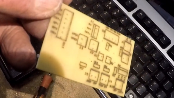
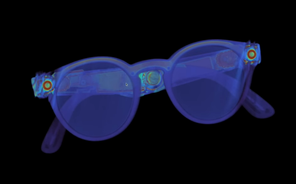
At first glance, the glasses don’t seem to be anything other than a normal pair of sunglasses, if a bit bulky But on closer inspection they hide a pair of cameras and a few other bits of electronics similar to the Google Glass, but much more subtle. The teardown demonstrates that these are not intended to be user-repairable devices, and might not be repairable at all, as even removing the hinges broke the flexible PCBs behind them. A rotary tool was needed to remove the circuit boards from the ear pieces, and a bench vice to remove the camera modules from the front frame. We can presume these glasses will not be put back together after this process.

Hidden away inside is a pair of cameras, a Snapdragon quad-core processor, capacitive touch sensors, an amplifier for a set of speakers. Mostly this is to support the recording of video and playback of audio, and not any sort of augmented reality system like Google Glass attempted to create. There are some concerning ties with Facebook associated with this product as well which will be a red flag for plenty of us around here, but besides the privacy issues, lack of repairability, and lack of features, we’d describe it as marginally less useful as an entry-level smartwatch. Of course, Google Glass had its own set of privacy-related issues too, which we saw some clever projects solve in unique ways.

Continue reading “Inside A Pair Of Smart Sunglasses”