Ken Shirriff Chats About A Whole World Of Chip Decapping

Reverse engineering silicon is a dark art, and when you’re just starting off it’s best to stick to the lesser incantations, curses, and hexes. Hackaday caught up with Ken Shirriff at last year’s Supercon for a chat about the chip decapping and reverse engineering scene. His suggestion is to start with an old friend: the 555 timer.

Ken is well-known for his work photographing the silicon die at the heart of an Integrated Circuit (IC) and mapping out the structures to create a schematic of the circuit. We’re looking forward to Ken’s talk in just a few weeks at the Hackaday Superconference. Get a taste of it in the interview video below.

Continue reading “Ken Shirriff Chats About A Whole World Of Chip Decapping”

TL084 die blocks

Ken Shirriff Found Butterflies In His Op-Amp

In 1976, Texas Instruments came out with the TL084, a four JFET op-amp IC each with similar circuitry to Fairchild’s very popular single op-amp 741. But even though the 741 has been covered in detailed, when [Ken Shirriff] focused his microscope on a TL084, he found some very interesting things.

JFETs on the TL084 op-amp

To avoid using acid to get at the die, he instead found a ceramic packaged TL084 and pried off the cover. The first things he saw were four stabilizing capacitors, by far the largest structures on the die and visible to the naked eye.

When he peered into his microscope he next saw butterfly shapes which turned out to be pairs of input JFETs. The wide strips are the gates and the narrower strip surrounded by each gate is the source. The drain is the narrow strip surrounding each gate. Why arrange four JFETs like this? It’s possible to have temperature gradients in the IC, one side being hotter than the other. These gradients can affect the JFET’s characteristics, unbalancing the inputs. Look closely at the way the JFETs are connected and you’ll see that the top-left one is connected to the bottom-right one, and similarly for the other two. This diagonal cross-connecting cancels out any negative effects.

[Ken’s] analysis in his article doesn’t stop there though. Not only does he talk more about these JFETs but he goes over the rest of the die too. It’s well worth the read, as is his write-up about the 741 which we’ve also covered.

[Ken Shirriff] Becomes A Core Memory Repairman (Again)

Lately, [Ken Shirriff] has been on some of the most incredible hardware adventures. In his most recent undertaking we find [Ken] elbow-deep in the core memory of a 50-year-old machine, the IBM 1401. The computer wasn’t shut down before mains power was cut, and it has refused to boot ever since. The culprit is in the core memory support circuitry, and thanks to [Ken’s] wonderful storytelling we can travel along with him to repair an IBM 1401.

From a hardware standpoint core memory makes us giddy. It’s a grid of wires with ferrite toroids at every intersection. Bits can be set or cleared based on how electricity is applied to the intersecting wires. [Al Williams] walked through some of the core memory history last year and we enjoyed hearing [Pamela Liou] recount the story of how textile workers consulted on the fabrication of core memory for the Apollo missions during her OHWS Talk in October. But giddiness aside, core memory has pretty much gone the way of the dodo having been displaced by technologies that take up exponentially less space.

Bad inductor (green housing has been dissolved away)

We chuckle at [Ken’s] mention of the core memory capacity for the IBM 1401. It has 4000 characters of memory built-in (with another 12,000 in an expansion box) and he goes on to detail that these are 6-bit characters on a machine that operates in decimal and not binary (hence 4k instead of the base-2 friendly 4096).

You may remember his work a few years back to repair core memory on the same model. The Museum has two 1401’s, which turned out to be a huge help in trouble-shooting this. After tracing out the control lines, the repair team began swapping cards between the working and non-working machines. They were able to bring it back online — establishing one of the green inductors was bad — only to be struck with a second fault in the power supply.

Get this, [Ken] comments that “the whole computer is pre-silicon”. When working through the PSU, some suspect transistors were replaced with germanium power transistors. Those may have been a red-herring, as a penciled-in fuse on the original schematics turned out to be the linchpin of the PSU repair. Buried deep in the assembly, replacing the designed-to-fail part let the ancient beast awake once more.

Machines of this quality were heavily documented, and the schematics make this type of trouble-shooting a lot more manageable. But it’s still as much an art as it is skill. Make sure to give [Ken’s] article a read, and look around at the other repair jobs he’s documented — keeping these machines in service is becoming wizard-level work and we love being able to follow along.

Ken Shirriff Takes Us Inside The IC, For Fun

[Ken Shirriff] has seen the insides of more integrated circuits than most people have seen bellybuttons. (This is an exaggeration.) But the point is, where we see a crazy jumble of circuitry, [Ken] sees a riddle to be solved, and he’s got a method that guides him through the madness.

In his talk at the 2016 Hackaday SuperConference, [Ken] stepped the audience through a number of famous chips, showing how he approaches them and how you could do the same if you wanted to, or needed to. Reading an IC from a photo is not for the faint of heart, but with a little perseverance, it can give you the keys to the kingdom. We’re stoked that [Ken] shared his methods with us, and gave us some deeper insight into a handful of classic silicon, from the Z80 processor to the 555 timer and LM7805 voltage regulator, and beyond.

Continue reading “Ken Shirriff Takes Us Inside The IC, For Fun”

[Ken Shirriff] Demystifies BeagleBone I/O

If you have ever spent a while delving into the bare metal of talking to the I/O pins on a contemporary microprocessor or microcontroller you will know that it is not always an exercise for the faint-hearted. A host of different functions can be multiplexed behind a physical pin, and once you are looking at the hardware through the cloak of an operating system your careful timing can be derailed in an instant. For these reasons most of us will take advantage of other people’s work and use the abstraction provided by a library or a virtual filesystem path.

If you have ever been curious enough to peer under the hood of your board’s I/O then you may find [Ken Shirriff]’s latest blog post in which he explores the software stack behind the pins on a BeagleBone Black to be of interest. Though its specifics are those of one device, the points it makes have relevance to many other similar boards.

He first takes a look at the simplest way to access a Beagle Bone’s I/O lines, through virtual filesystem paths. He then explains why relying so heavily on the operating system in this way causes significant timing issues, and goes on to explore the physical registers that lie behind the pins. He then discusses the multiplexing of different pin functions before explaining the role of the Linux device tree in keeping operating system in touch with hardware.

For some Hackaday readers this will all be old news, but it’s safe to say that many users of boards like the BeagleBone Black will never have taken a look beyond the safely abstracted ways to use the I/O pins. This piece should therefore provide an interesting education to the chip-hardware novice, and should probably still contain a few nuggets for more advanced users.

We’ve seen a lot of [Ken]’s work here at Hackaday over the years, mostly in the field of reverse engineering. A few picks are his explanation of the TL431 voltage reference, a complete examination of the 741 op-amp, and his reverse engineering of the 1970s Sinclair Scientific calculator.

We appreciate [Fustini]’s tip on this story.

BeagleBone Black image: BeagleBoard.org Foundation [CC BY-SA 3.0], via Wikimedia Commons.

[Ken Shirriff] Explains The TL431

[Ken Shirriff] had to get down into a bit of semiconductor physics to give us an explanation of the TL431, which he calls “the most common chip you’ve never heard of”. [Ken] may well be right about the TL431. Even Texas Instruments can’t nail down a single name for it. Their page for the part calls it a “Adjustable Precision Shunt Regulator”, yet the datasheet is titled “Precision Programmable Reference”. You’d think they’d have figured this out by now, considering the TL431 was launched in 1978.

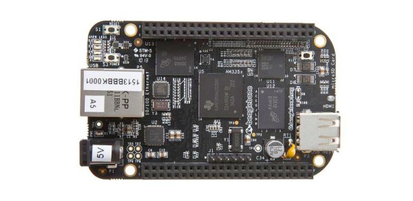
TL431’s can most often be found hiding in switching power supplies. The Apple II switcher had one, and many current ATX supplies have 3. Uninformed parts scroungers may miss them, as they often hide in TO-92 or SOT-23 packages. The TL431 is no transistor though. The TL431’s operation is actually pretty simple. When the voltage at the reference pin is above 2.5V, the output transistor conducts. When the reference voltage falls below 2.5V, the device stops conducting. In a power supply, this operation would help the control electronics maintain a stable output voltage.

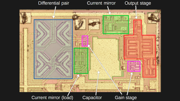
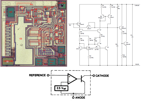
The real subject of [Ken’s] article is the layout of the TL431 on its silicon die.  Rather than bust out the fuming nitric acid himself, [Ken] uses some of [Zeptobars’] decapped chip images. Inside the TL431, [Ken] discovers that transistors aren’t made up of the three layer NPN or PNP sandwich we’ve come to know and love. In fact, the base isn’t even in the middle. Transistors, including the BJT’s used in the TL431, can be assembled in a nearly infinite number of ways.

[Ken] moves on to the resistors and capacitors of the TL431. The capacitors are formed two different ways, one as a reverse biased diode, and the other as a more traditional plate style capacitor. The resistors include fuses which can be blown to slightly increase the resistance values.

The takeaway from all this is that once you get down to the silicon level, it’s a whole new ball game. Chip layout may look a bit like PCB layout, but the rules are completely different. [Ken] mentions that in a future blog he’ll go into further detail on the operation of the TL431’s bandgap voltage reference. We’ll be watching for that one, [Ken]!

[Ken Shirriff] Completely Reverse Engineers The 1974 Sinclair Scientific Calculator

Wow. Seriously… Wow! The work [Ken Shirriff] put into reverse engineering the Sinclair Scientific is just amazing. He covers so much; the market forces that led [Clive Sinclair] to design the device with an under-powered chip, how the code actually fits in a minuscule amount of space, and an in-depth look at the silicon itself. Stop what you’re doing and read it right now!

This calculator shoe-horned itself into the market when the HP-35 was king at a sticker price of $395 (around $1800 in today’s money). The goal was to undercut them, a target that was reached with a $120 launch price. They managed this by using a Texas Instruments chip that had only three storage registers, paired with a ROM totaling 320 words. The calculator worked, but it was slow and inaccurate. Want to see how inaccurate? Included in the write-up is a browser-based simulator built from the reverse engineering work. Give it a try and let us know what you think.

Now [Ken] didn’t do all this work on his own. Scroll down to the bottom of his post to see the long list of contributors that helped bring this fantastic piece together. Thanks everyone!

[Thanks Ed]