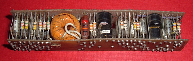
What you see above is a cordwood circuit, an interesting circuit construction technique from before the days of integrated circuits. The circuit consists of two circuit boards arranged parallel to each other with components holding them apart. This was, for its day, the densest circuit construction technique, used in everything from late 50s aerospace tech to huge computers that filled rooms.
The folks over at Boldport have a love for interesting PCBs and are apparently aficionados of antiquated tech, leading them to create their own cordwood circuit. Here’s the best part: it’s a kit, without assembly instructions.
The cordwood puzzle assembles into a bunch of LEDs that will light up when power is applied. Not much, but there’s a few FETs in there that allow you to control them all individually with a microcontroller. The real fun is trying to assemble the kit: both sides of the cordwood circuit are identical, meaning there’s going to be holes that aren’t meant to be filled, components that will need to be soldered, and most likely a bit of swearing.
Still, this is an exceptionally small circuit for something using this construction technique. If you know of a denser and more modern cordwood circuit out there, leave a note in the comments. If you want to know what the kit looks like when it’s built, [Phil Wright] has your back.


I haven’t run across a cordwood circuit in a long time, but I do remember seeing some in my younger days.
I might just have to come up with a circuit to build cordwood style, just to explore the technique.
I bet someone will do an Arduino clone in this fashion
That’s a great idea :)
Four boards with a TQFP? It CAN be done! One side to each board…. need to make custom footprints… autorouting will be nearly useless… Rubik’s cube and aspirin come to mind. Would be MOST impressive though.
I’m getting a migraine just thinking about it.
…
I love it
Four? Why not six and make a cube?
If the opposite pair of the cordwood boards were to made into a double side PCB without plate through holes, one could fit 0603 parts right in the hole! 0603: 0.06″ x 0.03″, would fit in 0.031″ dia hole on a 0.062″ thick PCB.
Making rectangular holes for SOT-23 would take a bit of work. :P
I think it is amazing just how many images are recycled on the internet. That picture of the “cordwood board” is also on Nixieguy’s blog from February 2014. you can see it half way down the page:
http://electronicmercenary.wordpress.com/2014/02/
Maybe he stole it from them?
sorry, I forgot to mention, Kristina featured his “tiny improvised grinder on 03/12/2014
Nice immediate jump to blaming somebody there. The image is from the Printed circuit board article on Wikipedia.
This is a file from the Wikimedia Commons. Information from its description page there is shown below.
Description
Electronics module exhibiting w:cordwood construction. I took this picture of an object in my possession on February 3, 2006.
Date February 3, 2006
Source Self-published work by ArnoldReinhold
Author ArnoldReinhold
There are some very nice looking pcbs on that site
I’m vege-cursing just imagining having to change out those Mil-Spec Axial Electrolytic capacitors after they dry out.
I feel like shorting might have created an issue with this design at some point. Wiggle either board to much and leads start touching.
I don’t think it was as big of an issue you might be lead to believe. Not when you get squarely into the realm of hundreds of components. Eventually, you get enough of those fragile thin leads working together to make something fairly tough. If you really wanted to, small dowels or similar can be worked in to add strength. Of course a deliberate impact from the side with a screw driver will probably screw it up, but that’s true for any circuit.
I seem to remember an old model rocketry magazine featuring just such a design for a homing beacon to be inserted into model rockets. The compactness and the board layout lent itself well to be slipped down into a tube.
I get frustrated if I solder a component backwards and have to fix it on a normal PCB. Imagine finding out a component in the middle of the board was reversed!
I’d have to learn some new cursewords to deal with that situation.
Look at nixieguy’s blog http://electronicmercenary.wordpress.com . He regularly gets in boards that have SOP chips wanting to pretend to be QFP. Also boards with buddyed up smt resistors and capacitors. Though he does manage to mangle a few LEDs all by his lonesome.
This is one of the main reasons why this technique was abandoned nearly everywhere long before SMD became available. Errors aside, just imagine servicing a board assembled like that. Last time I saw one of these boards was a computer discrete RTL/DTL board I got in some surplus store in the mid 70s and soon dismantled to build other things with the components.
Just imagine you are repairing a 15x15cm cordwood board, you have the schematics and everything, know which part is under which pin and suddenly you realize a transistor is fried in the middle of the PCB and is sourrounded by a wood of other components. ==> FUUUUUUCK
Reminds me a bit of a Cray 2 module I have, with 8 boards sandwiched in around 1″ of space. Here’s a description:
Cray-2 modules have 8 boards, each individual board has 6 printed layers inside, one of which is a clock layer, for a total of 48 printed planes per module. The 8 boards for both logic and memory modules were identified as abc, def, ghi, jkl, mno, pqr, stu, vwx. Vertical pins connected the boards together-really amazing packaging and the modules were submerged in fluronert to dissipate heat. We hand tested each diode with a scope and matched diodes with the same drop per power supply. This was truly a hand-made supercomputer.
I worked at Bendix in the 60s on the Talos missile, we laid out 1-2 a day. At Northrop on the SR-71 we designed multilayer cordwoods. They were drawn 4/1 on mylar and each layer, up to 4 per side showed the component hole and a line indicated the trace. one sheet was the assembly, bill of material and each layer. the drawing was reduced to 1/1 and the film was cut to size, and holes were punched. components were inserted and a wire was welded from comp lead to lead per the line on the film. Then another layer of film was added and so on. In the end the module was tested and dipped in conformal coating. Some modules were as large as 2×2 in. and up to 8 layers, 4 top, 4 bottom. Certain comp leads were left long (not shown in the illustration) and plugged into multilayer boards. These modules were repaired as needed. These boards ran in circulating silicone oil (coolinol 40) for heat dissipation. “O” one more thing, some modules were just rows of 14 and 16 pin flat packs, 10 to 14 per row, we never tried dip’s.
Good luck reworking that clusterf*ck Chuck is all I have to say about this.
THANK YOU! I remember seeing this style of construction years ago, and have been trying to remember what it’s called! Cordwood Construction. I’ve been wanting to design a circuit to implement using this technique.. I’ll do it at some point :D