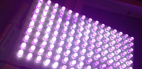
Among the projects that define electronic design, a UV exposure box is right up at the top of the list. These boxes shine UV light on a work piece and are used for everything from exposing photosensitive PCBs to erasing EPROMs. [carlolog] decided to build his own and ended up with a fairly impressive array of ultraviolet LEDs perfect for making PCBs or tanning the back of your hand.
One important thing to remember when making large arrays of LEDs is current consumption and power needed to light the device up. [carlolog] naive assessment of how much power would be required used a 12 volt supply with 135 LEDs and 135 resistors, wasting a lot of energy and producing 24 Watts of heat.
Of course this power consumption can be reduced by putting a few LEDs in series, so [carlolog] wired 3 LEDs together with a 150Ω resistor. This array requires just over 11 Watts and consumes less than 1 Amp; perfect for a desktop UV box.
The enclosure for the box was crafted out of three Ikea photo frames, and a small timer circuit powered by an ATmega8 was added. Now whenever [carlolog] needs to wipe an EPROM, he can put the chip in the box, set the timer, and walk away.
A very nice build, but when dealing with a lot of UV we must remind our readers: do not look into the UV array with your remaining eye.


I like the warning, Hackaday definitely knows it’s audience. Well done/useful build!
Dealextreme has mains “20W” powered constant current led drivers for about $10 or even cheaper.
If you’re just after saving money then it’s worth knowing that UV lamps for drying painted fingernails (on eBay) are a lot cheaper that those for exposing PCBs. I’m not knocking the project, as I know that’s not usually why most of us build / hack stuff.
Also, correct me if I’m wrong (like you guys wouldn’t!) but I believe the wavelength for erasing EEPROMs and exposing PCBs are different, so make sure you get the appropriate lamp / LED for the job.
+1 on the warning.
Oxfred you’re quite right, you may have a hard time erasing EPROMs with the setup above. You would want a UV-C based light, like was posted on Hackaday in the past. Although be aware that some do make UV-C LEDs now (check ebay), some are using them to purify water. Please be aware that UV-C can have even more harmful affects on your skin and eyes than UV-A (heed the Hackaday warning!).
I think i saw that warning on a cheap chinese laser-cutter…
Hate to break it to him, but they ain’t UV LED’s. True LED’s ain’t purple!
Those look like “blacklight” LEDs indeed.
Has it been tested for PCB purposes already?
From wikipedia: “LED
Ultraviolet light can be generated by some light-emitting diodes, but wavelengths below 380 nm are uncommon and the emission peaks are broad, so only the very lowest energy UV photons are emitted, within predominantly visible light.”
To add: http://www.mgchemicals.com/tech-support/instructional-guides/prototyping-faq-exposure/#q1
this particular manufacturer provides a lamp that is at 375nm for their boards.
Hi Elias,
I used the array to impress the timer pcb, 6 minutes at full power. Seems that it worked without problems. The pcb board was from Bungard. I think that the wavelenght of those leds is between 400 and 450nm.
It’s an RGB picture, the UV of the original LED has been lost in translation.
Anyone know if these types of UV lights would provide the right spectrum for UV-curable inks?
I believe they will. I use the same thing for curing screenprinting emulsion to make my own screens for printing t-shirts.
yes they do, i made a similar UV exposure box and it is good for both curing an pcb mask ink and for photosensitive pcb board.
get UV tube for 10$, use it, problem solved without soldering over 9000 LEDs.
jkop, what does the multimeter say about his power level???
i have used some 400 nm “UV” leds for my own pcb exposure box. First things first he will probably have problems with his exposure because he is very close to the actual surface, my circuit boards had hot spots on the photoresist because of this. But the 400 nm ones cured a green uv soldermask that I bought off ebay very well, but the blue one was another story and took twice the exposure time and still was not as cured as the green was.
Slightly off topic. does anyone know of a supplier of narrowband VUB around 310nm that aren’t a kings ransom? anywhere from 300 to 320nm would do. thanks
I also am looking for 310-315nm leds or lasers I can not find any unless you want to buy over 300.
Regular CFL bulbs work fine for exposing PCB. Been doing it a long time, takes about 12 minutes for a board and you can get the bulbs everywhere. I use the ~100w incandescent , 23W consumption versions made by sylvania. I position the bulb in one of those desk lamps about 10 inches above the board.
Well worth knowing! Does it do EPROMs too?
I’m doing this too right now, only with wide angle LEDs. I think a hexagonal pattern is better for even illumination (because distance between any two neighbor leds is roughly equal). I already tried with regular UV leds and it was pretty good (but had to be pretty far from the pcb not to show any ‘light rings’), those wide angle versions are a huge improvement.
And to all the haters here – those UV leds do emit some bluish-purple light visible to the human eye but they expose pcbs just fine, in fact a LOT faster than UV tubes at fraction of the power. And did it even occur to you that those digital cameras have no problem capturing UV light ?
i cant remember exactly what, but i put a filter overtop of a webcam that has the UV/IR filter removed and pointed it at my flourcent-tube-backlit-LCD… (seperate monitor and computer) it was glowing dimly, but i could NOT see ANY video. so is it safe to say that the LCD only blocks visible light when video says to, but UV/IR goes straight through???
i bought one single UV LED that costed ~5$
if i shine it directly on my skin, it starts to feel like a sunburn. as soon as i shut it off it feels better.
PS: it gives off just as much purple light as a high brightness purple LED. but this one is a weird purple-blue-lavender and hurts/burns skin WAY more then the purple LED.
they both trigger phosphors ect and make colored glowey things glow. picture tube face… eerie
PS: it gives off just as much purple light as a high brightness purple LED. but this one is a weird purple-blue-lavender and hurts/burns skin WAY more then the purple LED.
Based on WHAT?
Your vision or a calibrated measuring device?
you really have to watch these cheaply made LED devices from China, they dump a significant amount of radiation outside the visible spectrum, because the dyes they use are shitty or contaminated.
So you can easily end up with eye damage, even though the devices don’t look bright.
WAIT JUST A MINUTE…
Did you just imply that LED’s use DYES to make the different colors of light?
PLEASE, for the LOVE OF GOD tell me that is not true.
And by that I mean PLEASE TELL ME that you don’t think LED’s use dyes. LOL!!!!!
To me, even though this uses LED’s instead of the easier, cheaper, better-working fluorescent solution, this still needs a collimator for a good quality PCB that has really fine traces.
I bought some UV five junction
diodes a while back with major
wavelenghth spread between units.
A good test is to get a broken but
still LED’s UV laser diode, decan it
then shine your diode at it.
Monitor the voltage to determine
both wavelength and power level.
With the typical broken PHR803
or burner diode it works well.
Somewhat works with a KES400AAA
but not so well, smaller area.
Add aixiz lens to increase efficiency.
Whoops. Spell check snafu.
Also worth a try, use a broken 780 or 808
as an infrared version of the above./
It really works well and is FAST!
great project, i might make a new pcb exposure with LED.
I made a DIY UVA box for pcb exposure from a cheap used facial sunlamp:
http://techmind.dk/elektronik/diy-lyskasse-til-printfremstilling/
It works great.
I newer made a topplate with hinges and so, but works well with a aluminiumplate on top of foam plate ;)