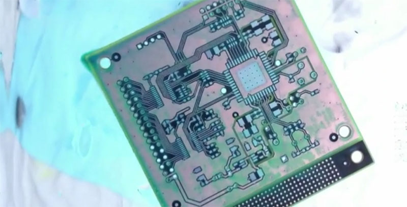
The surest way to reverse engineer a circuit is to look at all the components, all the traces between these components, and clone the entire thing. Take a look at a PCB some time, and you’ll quickly see a problem with this plan: there’s soldermask hiding all the traces, vias are underneath components, and replicating a board from a single example isn’t exactly easy. That’s alright, because [Joe Grand] is here to tell you how to deconstruct PCBs one layer at a time.
Most of this work was originally presented at DEFCON last August, but yesterday [Joe] put up a series of YouTube videos demonstrating different techniques for removing soldermask, delayering multi-layer boards, and using non-destructive imaging to examine internal layers.
If you’re dealing with a two-layer board, the most you’ll have to do is remove the soldermask. This can be done with techniques ranging from a fiberglass scratch brush, to laser ablation, to a dremel flapwheel. By far the most impressive and effective ways to take the solder mask off of PCBs is the way the pros do it: chemically. A bath in Magnastrip 500 or Ristoff C-8 results in perfectly stripped boards and a room full of noxious chemicals. It makes sense; this is what PCB houses use when they need to remove solder mask during the fabrication process.
Removing a solder mask will get you the layout of a two-layer board, but if you’re looking at deconstructing multi-layer boards, you’ll have to delaminate the entire board stack to get a look at the interior copper layers. By far the most impressive way of doing this is with a machine that can only be described as gently violent, but passive, imaging techniques such as X-rays, CT scanners and other sufficiently advanced technology will also do the trick. Acoustic microscopy, or Acoustic Micro Imaging, was, however, unsuccessful. It does look cool, though.
Thanks [Morris] for the tip.


You can go to the local vet and x-ray it.
– “My pet ‘Chip’ is sick, i need him X-Rayed”
– “That looks like a furby, they are not live animals”
– “Please doc! He’s real sick!”
‘He’s part Borg.’
Lo-Cute-Us
Just date that girl working at the local vet!
Nope… it is not reliable.
What you actually need is a ‘sister’ who has access to an MRI scanner, so that you can cross section the PCB, just need to ensure it is really flat.
“[Joe Grand] is here to tell you how to deconstruct PCBs one layer at a time”
For a second there I thought he was showing how to deconstruct different layers of a multi-layer PCB. That would have been awesome-er !
That’s what he’s doing ! Just look at the youtube playlist ;-)
One quick and dirty technique, shown in the later half of this video:
https://www.youtube.com/watch?v=jiPGTSTCREY
is to grind down to the next layer of copper, then put the board on a flatbed scanner. Repeat until the board disappears into a pile of fiberglass dust.
If you’re ok destroying the part, there’s a whole lot that can be gleaned from a really precise cross section analysis.
I’m reminded of how The US National Library of Medicine performed the same “analysis” on a human being…kinda gruesome, but the end result is very cool!
http://www.nlm.nih.gov/research/visible/visible_human.html
yes, he does? sanding it down with sandpaper or a surface grinder worked beautifully. He removes one layer to expose the next. What is there not deconstructing about it?
The only drawback to surface grinding is that the copper traces tend to gum up grinding wheels. If it isn’t dressed often enough, the wheel will catch and tear up the board. Otherwise, the 0.0001″ tolerances of a surface grinder are hard to beat.
That small amount of copper is not a problem with a surface grinder, especially with a CNC creep grinder with the coolant on like he’s using, and if the wheel is clogging or glazing up you’re using too hard of a wheel for the material you’re grinding. That’s why Norton and the other abrasive manufacturers have differing compositions of wheels. One of the softer and more porous wheels would probably do the trick, IIRC what we used for grinding copper and brass EDM electrodes on manual surface grinders, a ASA SC/60J probably would be a good start, that’s a Silicon Carbide 60 grit medium hardness vitrified grinding wheel that would be good for taking off about 0.002″-0.004″ of stock per pass on non ferrous stuff like copper or PCB material and the silicon carbide grit should stay sharp enough to cut the fiberglass but you’d probably need to play around with the structure of the wheel to reliably grind through the fiberglass, that’s the next number in the grinding wheel code. A little wax on the wheel helps too, like the sticks of wax for bandsaws. We did a lot of dressing fancy and complicated shapes into the electrodes, so we used a much higher grit than you would use for just grinding something flat, like a 180 grit to hold a 0.0035″ radius
I’ve always wondered what it would take to just separate the layers themselves, essentially undoing the lamination process.
I’ve thought about that too, but I think all the little metal cylinders that make up the vias would pretty strongly hold the layers together.
So it would take drilling out all the vias and through-hole cylinders before trying to separate the layers.
Seems doable, but what would you use to get the layers apart? Just heat in an oven? 500F or what do you think?
I don’t think it works that way. Delamination happens because the epoxy in the prepreg breaks down, forms gasses and essentially pushes the fibers off of the core. It doesn’t happen just at the boundary between layers – it happens all through the epoxy. If you leave it at a delamination point long enough to try to make the *entire thing* delaminate, the prepreg will basically be entirely broken down – especially around the places where you just fractured the heck out of them with the drill.
Why does the prepreg breaking down matter? Think about a 4 layer board – it’s “prepreg/core/prepreg”. Trying to peel off the “top layer” will just rip it and the nearest inner layer to shreds, since the thing it’s supposed to be laminated to is a broken-down fiber mess.
Sorry, I should clarify – the delamination happens at the boundaries, obviously, but the breakdown occurs throughout the thing.
Yeah, I think an oven might work. Maybe throw some ice on one side right after it comes out of the oven to cause a enough lateral stress to pop the layers apart. Maybe use a similar technique to get the vias out as well (depending on the thermal expansion rates of the vias vs. the board itself). I wouldn’t be too concerned about stretching the board since the point is to figure out where things go, not put it back together.
With today’s surface-mount devices and serial interfaces, there aren’t many through-hole cylinders left. As for vias, I have a couple ideas:
*reverse the electroplating process on via created with that method by running current through them in a container of water
*heat up the board to liquify any vias that are made by filling the holes with solder
*Heat up the board so that solid vias come loose
*Heat up the via so that it tubular via crush themselves against the board and become loose when they shrink back down to their proper size
*On some of them, it might be possible to just apply a bit of pressure to push some of them out.
These are just ideas, I’ve never ran the number to see if they are possible… If anyone knows if these are crazy / stupid, let me know, I’m always willing to learn more.
A little ‘crazy / stupid’ but do take a look at some pcbs, the material properties and how a multilayer PCB is made…..then you’ll know why those ideas are ‘crazy / stupid’ :-)
Alright. But what about non-destructive ways to do it ?
X-rays are about the only non destructive way to investigate, and that in itself isn’t very good. It can handle 3 layers before things get messy. If internal layers have copper filled ground and power planes, it will severely block the radiation from penetrating. Plus it’s hard to easily tell which layer a trace is on. Think of a ball power cords you pull out of your parts bin. You can see the wires but tracing where they all go is going to be a real pita. The point here is that tracing the circuit is much simpler if you have a spare unpopulated board and a belt sander. If it’s a bad board, desolder the parts, grind down each layer, and document it for the community. You would be doing everyone a great service.
Nope!!!
MRI……
“These techniques will only take off the solder mask, a great solution if you have to reverse engineer a single- or dual-layer board. To reverse engineer a multi-layer board, you’ll have to look into X-rays, CT scanners, or other sufficiently advanced technology.”
Actually, my research and the associated videos cover all three phases of PCB deconstruction:
– Solder mask removal (access to top and bottom copper layers)
– Delayering (access to inner copper layers of a multi-layer PCB, typically destructive)
– Imaging (access to inner copper layers of a multi-layer PCB, non-destructive)
Solder mask removal is only the first step in the process and the delayering and imaging steps are arguably more interesting. The end goal is to obtain clean images of each PCB layer that can then be used for further reverse engineering. Full results of my various attempts are documented on my site (linked in the original article) and I’m working on some new techniques. Some of my current favorites include surface grinding and 3D/CT X-Ray.
Enjoy :)
Joe
You are right but please cut Brian some slack. He has to write all of those sentences multiple times a week about various complicated stuff – most of which are very cool btw. Let’s not focus so much on the technicalities here (like how X-ray imaging can be passive, etc).
Now we just need a reliable method to identify all of those cryptically labeled SMT parts!
Usually you can make an educated guess as to the function of those cryptically labeled SMT parts. I find I have the most problems with those epoxy blobs. Sometimes you get lucky and under the blob is an SMT chip, although most the time it’s a bare die wire bonded to the board. Sometimes there are debug points on the board, and you can figure out what the chip is. Although that doesn’t do much good if it is a custom ASIC.
I’ve had some success using acoustic microscopy on boards. It’s not fast though and can be very finicky. I can’t really tell much about what he is doing from that short video that is linked.
And of course you can always desolder everything and electrically trace the board connections, then run the netlist through an autorouter program if you want a low resource ballpark.
the colored solder masks I’ve had on my PCBs are quite transparent in the infrared. A modified webcam (bandpass filter removed) and an incandescent lamp should be good enough for a start
COOL! Never thought about that!
Amazing the number of things that a shift in wavelength can reveal. I’ve often wondered why someone hasn’t made an actual product (Like a cheaper version of a GoPro) with the ability to discern basic images in, say near-IR and Ultraviolet? I know that a good DSLR and the right filters can do this, but it’s kinda pricy…
A hundred-dollar cheap point and shoot with the right filters? I’d buy one in a heartbeat. Much like programs like Word and Excel becoming the “Killer App” in the computer world and driving forward use and production, we need something along those lines to make this useful…Verifying sunscreen application, for example?
http://upload.wikimedia.org/wikipedia/commons/0/0d/UV_and_Vis_Sunscreen.jpg
Wasn’t there a hubbub about a camcorder with a UV filter that rendered many swimsuits transparent?
Ohm it out.
Take each pad for each device and figure out which pads are electrically shorted together. Might be tedious but I could do this at home without x-rays or acid or solvent. Wouldn’t give you the layout to reconstruct but you would get the schematic.
What about removing components and then probing every pad/node so you can map the connections, would this be practical.Probe a single node on one side then make up a wide probe from say a conductive brush, then sweep it across both sides to find any continuity to that pad/node.
When I say “wide probe” I mean a multiprobe (so each conductive bristle is ineffect an indvidual identifiable probe)
Isn’t it sad that “Reverse Engineering” (which is a valid form of engineering IMHO) wouldn’t be necessary if we made “Open Source” the rule of the land? We are already deep into a world where, due to substantial effort being placed on replicating a competitor’s successful product that “proprietary”, hidden source design and code just means it’ll just take a bit longer to figure it out? And often, the engineers won’t get it entirely right?
Instead of clever people working on bigger and better they are instead working on cranking out more crap cheaper? So much so that E-waste is starting to be a serious environmental problem?
I decided a long time ago that at least in the arena of smartphones I refused to participate in the rat race. I would like to have a smartphone, but the fact that they change so quickly and are soo fragile galls me. I want a device that not only performs it’s essential function (communication) but also is robust and (GASP!) repairable!
Repairability means fasteners, not glue. Schematics, not secrets. Effing’ parts and a part chain. Code that can be examined and edited. Standards of interoperability that aren’t secrets. In short, DESIGNS that are publicly available, pretty much the antithesis of why reverse engineering is even needed.
Excellent article, BTW. I’ve even used some of these techniques myself (examining a competitor’s product to improve ours) and I’m no stranger to tearing things apart to see how it works.
I am from a different school of thought. Patents protect business plans which means a loan can be obtained from a bank because the bank knows I am protected to some degree. With a loan you can mass produce. If we went the way of piracy then technology would hold no value to investors or banks which means folks would not make a living doing this and the technology would not advance. Those who steal big ideas don’t mind doing so, because they are just smart enough to realize they aren’t ever going to be successful otherwise. Advances in drugs are the same way, if stealing were allowed then the money is gone and to follow that is the research, don’t let anyone lie to you about being noble in the tech or drug business, it is all about the money period. As far as smart phones go, it sounds like you are a bit of a grandpa in thought and your vision is short sighted. Something so complicated is going to be delicate and hard to repair at first, later on these phones will be indestructible which is the ultimate solution to being repairable or not. I think just reprinting a pcb is the best way to go about fixing one. Disposable crap is what they are. Most electronics are designed to be tossed like a Solo cup.
I realize this thread is over a year old. I just watched the video. As a personal project, I have a PCB for a vehicle ECU that I would like to reverse engineer to help me in repairing other ECUs since they are out of production. I watch the video and had an idea, a crazy idea, but an idea. Has anyone thought about adapting a tile cutter for the purpose of grinding layer of board away? It has lubricant supply, some models have a movable tray that can be move forward and back. The problems I can think of are adapting a thicker grind wheel and adjusting the grinding depth accurately. Like I said, just an idea.
Cool! :)
Similar to a shaper?
http://hackaday.com/2016/11/04/tools-of-the-trade-injection-molding/#comment-3255492
I cant believe how many typos I put in that last post. That shaper looks awesome. I was trying to think of a way to reproduce the way he used the wet grinding technique on more of a DIY scale. That shaper machine looks like cast iron or something super heavy and way over kill.