The competition between Intel and AMD has been heating up in the last few years as Intel has released chips fabbed with their 14nm++ process and AMD has been using TMSC’s 7nm process. In the wake of the two semiconductor titans clashing, a debate between the merits of 14nm++ and 7nm has sprung up with some confusion about what those numbers actually measure. Not taking either number at their face value, [der8auer] decided to extract a transistor from both Intel’s and AMD’s latest offerings to try and shed some light.
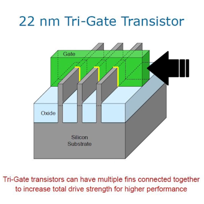
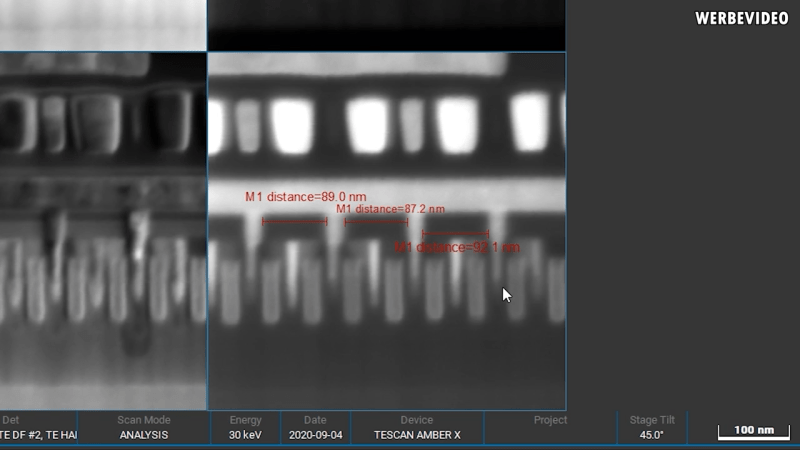
Much of the confusion comes from the switch to the FinFET process. While older planar transistors could be thought of as largely 2d structures, FinFET’s are three dimensional. This means that the whole vertical fin can act as a gate, greatly reducing leakage. It is this fin or gate that [der8auer] is after. On each chip, a thin sliver from the L1 cache was chosen as caches tend to be fairly homogenous sections with transistors that are fairly indicative of the rest of the chip. Starting with a platinum gas intersecting with a focused ion beam on the surface of the chip, [der8auer] built a small deposit of platinum over several hours. This deposit protects the chip when he later cut it at an angle, forming a small lamella 100 micrometers long. In order for the lamella to be properly imaged by the scanning electron microscope, it needed to be even thinner (about 200 to 300nm).
Eventually, [der8auer] was ultimately able to measure the gate height, width, spacing, and other aspects of these two chips. The sheer amount of engineering and analysis that went into this project is remarkable and we love the deep dive into the actual gates that make up the processors we use. If you’re looking for a deep dive into the guts of a processor but perhaps at a more macro scale, why not learn about a forgotten Intel chip from the 1970s?
Thanks [paulvdh] for sending this one in!


This article was way more fascinating than semiconductor fabrication videos.
FYI the specific microscope configuration used for final imaging wasn’t exactly your run of the mill SEM… it was actually a STEM (scanning transmission electron microscope). He mentions as much at 9:56
“courtesy of Werbevideo” is kinda funny because “Werbevideo” is “advertisement video” in German 😄
LOL. Bzw, peinlich. Fixed.
My computer design teacher (in the nineties) used to say “a cpu is a bunch of wires with some transistors” focusing on the fact that eacg transistor needs 3 wires and its the wires that connect everything. Thus i always figures the 14nm vs 7nm and 5nm were just the width of the wires connecting things
I’ll leave these here in case other people want to know more about the dimensions of the different process:
https://en.wikichip.org/wiki/intel/process
https://en.wikichip.org/wiki/technology_node
I would say history of the processes but most process nodes still have application somewhere. Anything 150nm and larger are useful in space outside of earths protective magnetosphere, because they require much less Graded-Z shielding (e.g. IBM/BAE RAD750 on the Perseverance rover launched 30 July 2020).
TSMC?
Taiwan Semiconductor Manufacturing Company – Pretty major semi fab house. AMD utilize them.
It’s a good thing Itnel is in competition with ADM! Speling errers iz herd too fidn. Apparently so are editors.
Having written thousands of pages of technical documentation, I know this to be ture!
TSMC is on the forefront of chip manufacturing and design. They recently announced 2NM. I don’t see Intel staying relevant much longer
You are right Intel have totally lost the marketing war, they need to change their process names to better compete with people who look at the node name and read meaning into it across vendors.
https://www.techcenturion.com/wp-content/uploads/2018/12/Transistor-Density-Comparison.png
3nm 291.21 MTr/mm^2 TSMC (estimate)
7nm 237.18 MTr/mm^2 Intel (estimate)
5nm 173.1 MTr/mm^2 TSMC (actual)
5nm 126.89 MTt/mm^2 Samsung (actual)
6nm 108.19 MTr/mm^s TSMC (actual)
10nm 100.76 MTr/mm^2 Intel (actual)
7nm+ 115.8 MTr/mm^s TSMC (actual)
6nm 112.79 MTt/mm^2 Samsung (actual)
7nm 95.08 MTr/mm^2 Samsung (actual)
7nm 91.2 MTr/mm^2 TSMC (actual)
14nm+++ ~90 MTr/mm^2 Intel (actual)
10nm 51.82 MTr/mm^2 Samsung (actual)
10nm 52.51 MTr/mm^2 TSMC (actual)
14nm++ 37.22 MTr/mm^2 Intel (actual)
sources:
https://hexus.net/tech/news/cpu/145645-intel-14nm-amdtsmc-7nm-transistors-micro-compared/
https://en.wikichip.org/wiki/10_nm_lithography_process
https://en.wikichip.org/wiki/7_nm_lithography_process
https://www.techcenturion.com/7nm-10nm-14nm-fabrication
https://semiwiki.com/semiconductor-manufacturers/samsung-foundry/8157-tsmc-and-samsung-5nm-comparison/
Sorry I did not sort them properly I have 2 lines below the 10nm intel node name that should be above it.
7nm Intel should be in production in 2022
3nm TSMC should be in production in 2022
The next big jump is not from TSMC, it will be from Samsung, with their GAA (gate around all), MBCFET using nanosheets. That will be good.
Semiconductor device manufacturing is an interesting topic.
And these video’s from Der8auer does highlight some misconceptions that people in general tend to have.
Though, it isn’t surprising that a lot of people look at the “x nm” and think that it is an actual size.
For process nodes above 100nm it kind of tends to be the case that it is the actual size of the smallest feature the node can reliably make.
But for nodes bellow 100nm it tends to be unrelated to the size of any feature on the chip. Or not, it depends on how we look at the statement. (We can measure the thickness of a coating, for an example the gate oxide layer. We can just as well make a transistor with a channel length that is a fair bit smaller than the smallest feature the process node itself can create in a photoresist, thanks to fancy doping techniques.)
In the end, it leads to a 7nm transistor’s smallest features actually measuring above 20nm. It is still ridiculously small though.
But to be fair, TSMC could release a transistor that has features that are 25-30nm and still logically call it a 4nm node if they desire. Since a manufacturing node isn’t about feature size, or length. It also refers to transistor density, power consumption, switching speed, etc…. The smaller number just denotes the next generation, following the semiconductor industry’s odd way of counting generations giving a rough 1.41x improvements. But companies count in different ways and look at different things for their definition for what they call x nm, so they don’t follow the same scale.
Ie, if you go to TSMC and ask for their 22nm node, then don’t expect it to be the same as Intel’s 22nm node, or Global foundry’s 22nm node, or anyone else’s for that matter. They are all different, having their own strengths and downsides.
It is simply confusingly unstandardized.
But Intel for an example couldn’t just go say that they now have 7nm, since the expected step up in performance/cost wouldn’t be realized. But the industry could just say, “X generation of our process” instead and stop using the confusing “nm” score.
Also, for everyone thinking one can just compare the size of features to determine that one is better than another, then no. There is a lot more nuance to semiconductor manufacturing than that. A smaller transistor isn’t inherently better for high speed logic.
> A smaller transistor isn’t inherently better for high speed logic.
True, the main issue limiting higher speed logic is cooling (Watts/unit area). Having more transistors, offers the opportunity to interleave between multiple circuits allowing each circuit double the time to cool down between uses.
We already use interleaving for memory in computers, where higher memory throughput is due to reduced waiting for memory banks to become ready for the operations. And in oscilloscopes where ADC’s are interleaved (e.g. HMCAD1511 where 4×250 MSPS ADC’s are time-interleaved to increase the sampling rate to 1 GSPS). In larger data centres dynamic thermal management/thermal load balancing is implemented, which is a nearly a kind of thermal interleaving.
More transistors might allow similar options at a chip scale. Imagine a hot CPU and a cold CPU with mirrored registers or even individual blocks of a CPU. It may seam ridiculous to add additional area primarily for cooling, but if it offers the potential for additional performance, why not.
The limit for high clock speeds isn’t purely about cooling either, latency and switching times eats up a lot of one’s time budget. To the point where a lot of logic needs to be built to have as few logic stages in series as possible, usually at the expense of having more logic stages in parallel to work with.
A simple example would be carry look ahead in a full adder. Since ripple carry is very slow….
Though, mirroring instructions and interleaving their operation is an approach to decrease power density while still getting good serial throughput. (One could run both sets at a lower clock, but that increases the time penalty of the instruction, even if we get more throughput. This can be beneficial for parallel workloads, but for more serial workloads it would often lower performance. (Ie, difference between GPUs and CPUs.))
If a given feature in an architecture can be interleaved or not is also a debatable question.
Registers for an example could be a bit iffy to interleave. Same for instruction decoding. (Since one cycle can be dependent on the prior cycle, so there it can be better to just have a hot spot on the chip than shuffling data between the two areas.)
All though, my statement about “A smaller transistor isn’t inherently better for high speed logic.” is actually about the fact that a smaller transistor can actually be worse, since its specifications are dependent on a fair few factors.
One good example would be when chip makers stumbled onto the problem of quantum tunneling, suddenly it didn’t matter much that one had a transistor or not, current just jump across regardless and increasing leakage rather phenomenally and hiking up power consumption without giving any additional performance. This is obviously bad for practically any application.
But leakage tends to be larger in smaller transistors in general, due to the shorter channel length being less high impedance compared to a longer one. Ie, there is reasons for why practically all “ultra low standby power” microcontrollers/SoC tends to use manufacturing nodes well above 100nm. Though at the expense of the transistors being a bit more power hungry when they cycle. (Though, one can use a hybrid approach where one just turns of the power delivery to the “high leakage” sections, getting the best of both worlds.)
Then there is also those times one has to drive a particularly long trace or an IO port, then it can be good to have a larger transistor able to source/sink more current.
But obviously, if one doesn’t have sufficient cooling, then the limits of interconnect latency and transition times aren’t going to be as important hurdles.