[Matt Keeter], like many of us, has a lot of network-connected devices and an oscilloscope. He decided he wanted to look into what was on the network. While most of us might reach for Wireshark, he started at the PCB level. In particular, he had — or, rather, had someone — solder an active differential probe soldered into an Ethernet switch. The scope attached is a Textronix, but it didn’t have the analyzer to read network data. However, he was able to capture 190+ MB of data and wrote a simple parser to analyze the network data pulled from the switch.
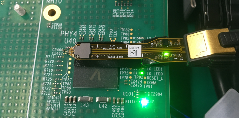
The point of probing is between a network switch and the PHY that expands one encoded channel into four physical connections using QSGMII (quad serial gigabit media-independent interface). As the name implies, this jams four SGMII channels onto one pair.
As is common in networking schemes, the 8-bit byte is encoded into a 10-bit code group to ensure enough bit transitions to recover the synchronous clock. The decoding software has to examine the stream to find framing characters and then synchronize to the transmitted clock.
What follows is a nice tour of the protocol and the Python code to decode it. It seems complex, but the code is fairly short and also executes quickly. The output? Pcap files that you can process with Wireshark. Overall, a great piece of analysis. He also points out there are other tools already available to do this kind of decoding, but what fun is that?
Wireshark can do a lot of different kinds of analysis, even if you aren’t usually capturing from a scope. You can even decrypt SSL if you know the right keys.


What’s the purpose of those little square copper islands on the PCB?
(very nice hack btw)
Most likely used to balance copper layers to prevent warping of the board in reflow. Probably done this way, because continuous copper pour is not desired in this application for some reason.
Your answer is likely correct, though decoupling capacitors existed at some points even in CPUs as PCB traces:
https://i.imgur.com/SBRSFDM.png
In skull trail they were replaced again for even smaller caps than you see already in this pic as SMD components. I suppose the PCB ones were disappointing at higher performance levels, but don’t know for sure.
Yup we call it copper thieving. Here’s a good article. https://pcbprime.com/pcb-tips/what-is-copper-thieving/#:~:text=is%20Copper%20Thieving%3F-,What%20is%20Copper%20Thieving%3F,distribution%20across%20a%20copper%20layer.
Usually, large blank areas on complex boards are filled with ‘Scavenging’ patterns to help balance the etch depth and quality during PCB manufacturing. When you do a lot of small precise copper work on a PCB, it becomes critical to balance how the board etches in the bath to make sure you don’t obliterate some of the tiny features by over or under etch. If you have a big open area on the PCB with nothing else to etch, the copper traces in that area have a real possibility to get over-etched and thus obliterated or end up the wrong width when finished (very bad for controlled impedance – for example).
It is a common practice at higher end board houses for complex boards, and the patterns vary and are added by them using analysis and tools tuned to their manufacturing process, after receiving your Gerber files. The addition of the copper scavenging pattern is usually only done upon approval from the engineers responsible for the project.
Always thought it was cute that 8B10B coding (as mentioned in the article) did so many jobs- ensuring enough transitions for clock recovery, DC balancing so AC coupling or transformers could be used, error detection/correction and sideband signalling using some of the extra codes
Nice, but i don’t even want to know the price of even only the active probe… :-(
>I configured the oscilloscope to collect 100M samples at 1 TSPS (tera-sample per second, 1012)
That can’t be true? The web says the fastest scope (article from 2018 but still) samples at 256GSPS, so…??
I think he’s using a Tektronix 6 Series B MSO and the datasheet says the sample rate is 25 GS/s to 2.5 TS/s interpolated, 6.25 S/s to 50 GS/s real time.
Uh ok, i was thinking real time of course.