
It’s yet another update to the Hackaday 68k, the wire-wrapped backplane computer that will eventually be serving up our retro site.
This is also a demo of Hackaday Projects, our new, fancy online documentation tool for all your adventures in making and tinkering. Did you know we’re having a contest on Hackaday Projects? Make something sci-fi, and you’re in the running for some really good prizes. There’s soldering stations, o-scopes, and a lot of other prizes being thrown at the winners. It’s awesome. First one to build a working Mr. Fusion wins.
In this update, I’m going to go over the beginnings of the video board, why Hammond enclosures are awesome and terrible at the same time, and some thoughts on turning this into a kit or product of some type. Click that, ‘Read more…’ link.
The Video Board
Like I’ve said before, I’m using the Yamaha V9938 video display processor as the graphics chip on this computer. It’s the easiest way I can get an 80×24 text mode – perfect for that *NIX goodness – and should be able to pull off some cool demoscene stuff. It’s pin compatible with the V9958, so I have that option, and it’s also fairly simple to interface to the rest of the computer:
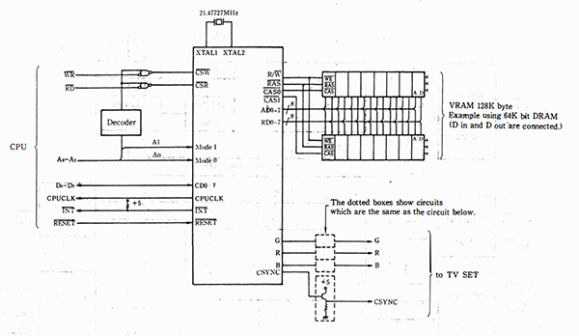
That’s from the V9938 Technical Data Book. Big PDF warning there. On the right side of that graphic is the DRAM interface for the video memory and the pins for video output. There are a few different configurations ranging from 16k of VRAM to 128k of VRAM. Of course I’m going with the 128k option, using a quartet of TMS4464 DRAM chips I picked up from Jameco. Here’s the schematic of the VRAM interface:
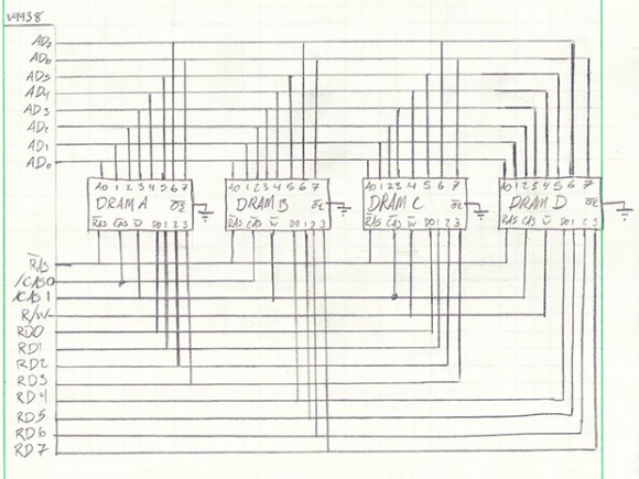
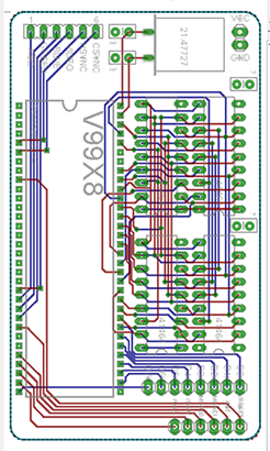 I don’t want to wire wrap that. It’s a lot of fiddly, short bits of wire. It’s also extremely simple and won’t be seeing any changes in its design. The solution to my laziness is, of course, to make a PCB.
Because the connections to the V9938 are just an 8-bit data bus and a few control signals, and the output is dead simple for composite output, this greatly minimizes the amount of wirewrapping I’ll need to do. Even if I tried wrapping a V9938, I’d run into a problem: the pin pitch isn’t 0.1″, rendering all my wirewrap adapters useless.
If you’re wondering about the physical size of the board, it’s just a wee bit larger than an Arduino. Yes, I know what you’re thinking, but a 128kB V99X8 will not fit on a standard Arduino shield. 16kB, maybe. In any event, when I get these boards back, I’ll have a go at driving it with an Arduino. Just because.
Mechanical Considerations
Yeah! Fancy Video!
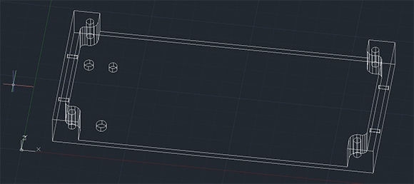
 I’ve never had any luck with Hammond enclosures. The die-cast aluminum guitar pedals? I’ve ruined dozens of them drilling holes for pots, switches, and jacks. The enclosure for the 68k is no different. It’s a beautiful case, no doubt about that, but I am cursed with a mystical ability to always mess up the drilling, painting, or some random thing when it comes to Hammond enclosures.
The original plan for this backplane + enclosure combo was to have a small extension board on the front (hence, “frontplane”) that broke out the power and reset lines so this computer would at least look the part of an early 80s homebrew computer. Also, having a power and reset switch on the outside of the case is a good idea anyway.
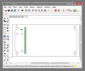 Because of the complete failure of my ‘frontplane’ plan with the stock front panel, I’m going for something much, much cooler: a custom CNC’d aluminum panel. Right now I have holes for a power switch, a reset button, and a 5mm LED for power indication.
The basic circuit for this frontplane is very simple: The lines on the backplane are broken out on a huge 2×32 pin header. There’s also a small three-pin header for the PS_ON and POWER_OK lines for the ATX power supply. Ground the PS_ON line with the switch, and the power… uh, turns on. The PS_ON line provides +5V when the power is on. Attach the LED to that.
The reset circuit is the same from the CPU board: a Maxim DS1812 supervisory and reset circuit in a single TO-92 package.
Creating the milled front panel and new, improved frontplane was an interesting exercise in mechanical design. First, I created the front panel as a 3D model, exported the top view as a DXF, and imported that into Eagle. Then, I took the board file for the backplane and overlaid the holes. Then it’s just a simple matter of removing the parts and traces from the backplane I don’t need – everything except the pin headers – and making a board.

So there you go. Fun adventures in mixing mechanical design with circuit board creation. This, like just about everything else relating to the 68k project, is up on the github.
Oh yeah, a kit
For some reason I can’t comprehend, a lot of people have asked if I’m going to make the 68k into a product, or at the very least a kit. I don’t quite understand the demand; the fun of homebrew computers is designing and building them.
That doesn’t mean I won’t entertain the idea. In its current form, though, a 68k kit would be absurdly expensive, take hours and hours to assemble – the RAM card alone would be three or four hours – and would have an extremely high number of unsatisfied buyers. It only takes one misplaced wire to screw the entire thing up, you know.
So, an improved, single-PCB kit is the only option. This is months and months in the future, but here’s what I’m thinking:
- Uses the currently-in-production 68SEC000
- Already assembled.
- A MiniITX or MicroATX motherboard form factor.
- Uses 30 or 72-pin SIMMs for the RAM.
- Some sort of expansion port.
- User-updatable ROM.
That last bullet is the sticking point. I’ve been turning this around in my head for a while, and I can’t come up with a good way of doing it. The problem is I need a small amount (~64kB) of EEPROM or Flash that can be accessed on a parallel bus. That means 15 address lines, 16 data lines, and control signals. I need a way of reprogramming this, in system, with few additional parts, cheaply.
The obvious solution is to throw a big FPGA in the system for address decoding, an SPI bus, and in-system reprogramming of the ROM. That may end up being the eventual solution to this problem, but I’m thinking there’s an even more clever and cheaper way of doing things.
I’ve toyed around with doing the whole ‘in system ROM reprogramming’ thing in a 6502-based retrocomputer, and it is possible by using a microcontroller and a bunch of shift registers to program the ROM. This takes up a lot of board space and is extremely kludgy.
Another solution would be something like this amazing retrocomputer that actually should be a product. It uses a 40-pin PIC microcontroller as the RAM, ROM, and ACIA. It is, without question, the most innovative project in the retrocomputing world for the past few years and presents an interesting solution to the problem of in-system ROM programming: just put the ROM on a big microcontroller.
Are any of these ideas the right solution? I don’t know, because I’m not designing this computer as a product right now. This problem has been bothering me for a while, and I’d love to hear some more ideas. In any event, there’s plenty of space on my ROM board to prototype some in-system reprogramming. Come up with a good idea and I might put it in.
That’s it for now. You can continue to follow the progress of the Hackaday 68k over on Hackaday Projects. Be sure to comment and give a skull to the project. Seriously, give the project a skull. I’m losing to [Mathieu]’s Mooltipass project in the skull department. I need more skulls.


OMG KIT!
I want.
Could you emulate to rom and run it from SD?
Oooohhh. There’s another one. Putting a ROM file on an SD card and accessing it via a micro….
Is it possible? Of course there is few limits like speed and that it is so new versus 68k but there could be something like microcontroller in between.
Modern SD is plenty fast enough for the needs of a 68K… if you could run it in 68K mode, In SPI mode (what most folks run when hacking around with SD cards), you’re limited to around 2Mb/s or so. It’s simple enough that this could be done with a simple microcontroller or even a CPLD. Keep in mind, back in the Mac days, Apple used the SCSI chip essentially as memory — the SCSI chip (they weren’t even using one of the better ones) controlled /DTACK directly.
Another option would be to use a bootstrap micro. Rather than having the micro proxy for the SD card, it could read that SD card and dump some number of sectors into RAM, then hand the reigns over to the 68K and shut itself down.
Of course, you don’t need much ROM, so why not just use NOR flash? You’ll need a flash-write routine for the 68K, and JTAG or something for the first programming, but that could be updated from files on an SD card via an all-RAM loader routine. Usually you want some boot-block code that doesn’t ever get overwritten, capable only of loading something from SD. So I’m still using SD, but it’s only as mass storage, not run-time ROM.
spi mode has no such limits. I have successfully run an SD card in spi mode with a 20 MHz clock, and the spec supports this
Cool! You are making good progress. :)
I was very suprised when people asked me for a Kit as well. Thus there will be a Kiwi kit in summer. :) Good luck!
CPLD comes before FPGA. And before that… 74F675A and 74F676. 16-bit parallel to serial, and 16-bit serial to parallel.
Program the Flash with something like a Bus Pirate, then use the chips to interface the Flash with the CPU.
http://www.classiccmp.org/rtellason/chipdata/74f675a.pdf
http://users.ece.utexas.edu/~valvano/Datasheets/74F676.pdf
>The obvious solution is to throw a big FPGA in the system for address decoding,
The obvious solution is to use a part with the SEC core and all of that stuff built in.. like I don’t know.. the MC68VZ328.
MC68VZ328 is obsolete and not produced any more, most part vendors are not carrying it anymore. Not to mention that it comes only in a 144pin TQFP or a rather big BGA package :(
Actually the older 68ks are easier to find on eBay and such than these Dragonballs, unless you want to desolder one from a Palm Pilot.
The address decoding can be trivially handled by a bit of glue logic or a small CPLD, e.g. XC95xxXL series from Xillinx, or if you really want to go old school, by a GAL device.
>MC68VZ328 is obsolete and not produced any more
They are the same around the same price as the SEC from parts brokers.. and there are trays of them on ebay.
Why not use a part like a NVSRAM from Maxim as the ROM ? like the parts on this page:
http://para.maximintegrated.com/search.mvp?fam=rtc&489=NV%20SRAM&tree=memory
You could sub-divide it into a fixed bootloader and an OS rom section.
A big FPGA? A tiny FPGA is enough to implement the entire 68K, V9938 and support logic. You can pick up an Altera Cyclone II based dev board (with 8K LEs), complete with VGA port, PS/2 keyboard port, 512KB of SRAM, 32MB of SDRAM, 8MB of flash ROM, an SD card socket, ADC and DAC chips, DS1302 clock chip and everything else you need for less than $80 on eBay.
Oh I so would love a kit version f this. That sad – why ot just mount the backplane on standoffs? That way you could chuck say an inch or two of space between it and the back wall of the case.
This might be a stupid question, so apologies in advance if this is the case, but what kind of video signal does it output? Or, in other words, what kind of monitor (TV?) can I connect it to? This might be a very good part for my experiments too, but I’d like to connect it to a VGA monitor ideally (even if this requires a couple more chips).
Check your monitor: your LCD monitor might already support 240p-over-VGA.
Just use a pair of 39SF040 chips for the upgradable ROM. These are 8-bit parallel flash memory. You erase and write them in 4K blocks, all in software, by writing some magic numbers at the right address. When not trying to write them, they behave just like a standard ROM chip. No need for any additional logic.
There are other flash chips like this, for example the AT29C040A, available in DIP packages for more wire wrapping fun. You can find them with different erase block sizes (256 bytes up to 16K) and also in smaller capacities if you don’t want 1MB of flash memory.
Instant gratification (well, sooner than later):
– minimig
– kiwi (if you don’t mind the 8-bit data bus)
Willing to wait and spend $$$:
– s-100-based 68000 board
I like the idea of using a micro to act as ROM, memory interface, I/O controller, etc…
An atmega2650 has 86 I/O pins available. That sounds like enough to do the job on a 68000.
A kit YES PLEASE, also a mini itx style 68k mainboard would be awesome
I would be interested in a kit but only if it uses modern day hardware and not a propeller chip. An Arm chip can create VGA.
I do like the idea of a kit. Single board… I don’t mind assembling unless there’s wire wrapping involved!
I would do so man enthrawling OS projects with this. Brian’s right that designing and building is a huge part of the fun. But I think seeing first hand what the original programmers were dealing with on a system like this is its own set of engaging projects.
>but I am cursed with a mystical ability to always mess up the drilling, painting, or some random thing when it comes to Hammond enclosures.
They have CAD files for the enclosure. Plan it out in CAD where you want to put hole. Print it out on paper, use a glue stick to attach the paper. Use a punch to mark the hole. If you are worry about wandering bit, drill a tiny pilot hole first and use masking tape to protect painted surfaces.
I use Black & Decker Bullet® Drill Bits for drilling. They have a finer pilot bit so they don’t wandering as much and they tend to give a cleaner cut that require less deburring.
FYI: There are already FPGA based 68xxx FOSS projects out there that have better specs with (closer to) modern day part and properly layout PCB.
MIST – Atari ST / Amiga fpga CLONE:
FPGA for 68xxxx, SDRAM, VGA, audio; uses ARM7 chip for peripheral and USB support. 199.99 EUR comes with preassembled PCB + a case!
Minimig – Amiga clone
FPGA for Amiga chipset + external 68xxx CPU/Microcontroller. VGA output. $163.51 US
How about using a type of flash memory which was designed for this explicit purpose: reprogramming and in-place execution? That is, NOR flash. For example, Micron M29F200. 48-pin TSOP, 20 dedicated address lines, 16 dedicated data lines, and control signals.
There is the issue of preprogramming those TSOP parts defore soldering them down for initial development as neither the 68xxx nor the parallel FLASH memory comes with easy in system programming interface.
There are sockets for them BTW.
Okay, it also comes in SOIC. There are widely available “clothes-peg” style SOIC adapters.
Depending on bus architecture (not familiar with 68k), it may also be possible to program them in-system, e.g. by adding an extension slot and making the programmer act as a bus master.
(By the way, I’m really disturbed how the cheapest way to access a flash memory through a parallel interface is, apparently, “throw in a big FPGA”. That’s literally the most expensive possible way except, perhaps, using an ASIC. ಠ_ಠ)
The problem for the parallel FLASH is the high I/O count required for programming, hence CPLD/FPGA/microcontroller solutions.
You could use 74XX595 for driving the address/data line and read back with a 74XX597 if you want to. Those chip have tristate output and you can put the 68xxx in reset and/or use bus request to force it to tristate its memory interface. You can Bitbanging the programmer on a parallel port. You can make a programmer for it in a slot with discrete, but by the time it is done, you are probably better off putting it in a FPGA/CPLD as you can reprogram them and add a lot more functionality for the system. Why stop at programming when you can have VGA or even the CPU core inside the FPGA?
I built a programmer with ATMega8 with V-USB in about 3 hours on a bread board with most of the time spent on stripping wires as I have already the PC host software, but I was building a quick & dirty programmer not a 68xxx computer in the first place! So easily to get side tracked and add complexity because the parts are being in system programming friendly.
What? To quote the article:
> The problem is I need a small amount (~64kB) of EEPROM or Flash that can be accessed on a parallel bus. That means 15 address lines, 16 data lines, and control signals.
I offered a chip which suits these requirements almost exactly. (It’s a bit too big, but I couldn’t find a small flash with a 16-bit interface. AT29C512-70JU is a 64k flash with a 8-bit one. Also, costs less than $1@1.)
What about using… the 68K CPU to do this?
The NOR-flash chips are designed to interface with a CPU bus. There are address pins, data pins, and the usual read/write signals.
Just preload the NOR-Flash (well, ok, to do this you need some other device that can program it) with some boot code that sets up the CPU, copy itself to RAM, then runs from there, configures a serial port, downloads a binary over xmodem and write it to the NOR-flash. And there you have your in-system programming.
Once you have a more complete OS loaded this way, you can use other ways to reprogram the memory as well (loading from whatever mass storage device you use).
>Just preload the NOR-Flash (well, ok, to do this you need some other device
>that can program it) with some boot code that sets up the CPU,
Indirect programming of a small serial bootloader to the flash using boundary scan on a CPLD or FPGA connected to the address and data bus would also work.
The way this project is done tells me that he is a person that rushes ahead – prefer to wire wrap a 68xxx machine instead of properly designing the whole system before implementing it. Having a fully debugged monitor/bootloader (e.g developed with a emulator) isn’t likely MO. There is going to be a dozen of crash/head scratching/burn cycles depending on the skill levels.
I would want a math coprocessor to be included with this kit. I like doing ridiculous floating point operators and vector drawings. I would be interested if it did come with the coprocessor. It looks nice, and I hope it’s successful.
Kit? Shutup and take my money!
Seeing the “moved everything .03 inches” on github reminded me of my little 3D print for a PIR sensor so much lol, it was actually around that size (.025 but rounded to .03) which was the radius of screw holes. I measured every aspect of the board for at least 24 hours. If I didn’t self-impose size constraints to save money it’d be a lot easier, but I (stupidly) thought it’d be easy to get any size screw and the box was just slightly off (so irritating). Having a 2nd go w/ it I could make it perfect. Just needed to drill it though.
I can’t get in your head as far as what you want for the enclosure, just take a deep breath and make cheap proto’s; because that’s the easy part. :p
You could have two separate sockets on the board, one that responds on 0xFF0000/0x0000 and the other at another address and just physically swap them when you want to use the other EEPROM for boot.
Or modify the reset vector circuit and add an AND gate with one input the BOOT signal and the other from a switch. The Switch would also control one or more bits on the addresses decoders for the ROMs.
This way to reprogram the BIOS, you’d send data to a specific address (Whichever one the secondary chip is listening on) then power-down, flip the switch, and power-on to use the other ROM.
Some modifications:
Add a couple flip-flops at a specific address and use the to toggle the WE pin on the secondary ROM and maybe one to control which ROM is the boot ROM (This Flip-flop should be battery-backed so that this value is preserved between power cycles)
I used 2 D type F/F to latch in the mouse buttons the /reset get deasserted. One of them drives the Bus Request for the 68000 and the other one on the 68020 accelerator to select the CPU. The other F/F was to select the ROM. You don’t need to power cycle the computer as reset (aka cold start) is a safe point to swap CPU or ROM as the system is initialized to a known state. There are non-volatile I/O chips if you don’t want dip switches. e.g. PCA8550 – “4-bit multiplexed/1-bit latched 5-bit I2C EEPROM DIP switch”
I would imagine that something like that can also be used to drive the upper address pin if you want a single set of ROM for fail safe/dual firmware. As [whitequark] pointed out FLASH do not come in small sizes these days.
In my first paying gig, I added a quad OR gate on my upper 4 address line to modify the ROM page of the boot rom in bootloader mode. The Fxxxx page of the ROM is used in bootloader mode regardless of what the actual ROM address was driven (aka aliasing), so all the vectors are mapped there. Bootloader is small, so 1/16 of the chip is not a limitation.
Copy the code from FLASH to RAM, you can then turn off the mapping signal and reprogram the ROM (as FLASH is not accessible in programming mode). You can write protect the bootstrap FLASH page by locking it if you want to.
The beauty is of this is that only 1 set of ROM chip is required and the whole ROM space is also accessible. 68000 requires 16-bit ROM, so you don;t want to add a 2nd set of chips.
I would look at NVRAM. It might be more parts, but should be simple. Have a battery and bootstrap the contents in somehow. Switch panel bootloader if you’re hc. Or just a separate microcontroller (raspi, ****duino…) board for the “flashing”.
As someone who’s currently attempted to build a 68k machine for myself, something I’ve wanted to do for many years, I’m a little disturbed by the suggestion that it should be a pre-made kit, or should contain microcontrollers or FPGAs or whatever.
I know we all do things for different reasons, but to me the fun of such a machine is that it’s built using relatively simple and reasonably period appropriate parts. If you put an FPGA or a microcontroller in it to emulate half the machine, you may as well go the whole hog and do away with all the other parts, it’s already become a completely different project by that point. People have built many different complete computers using almost only AVRs or PICs or Propellers or FPGAs, and I don’t want to put them down for it, but I think it’d be a shame to turn this 68K project into something else.
There are a million ways I could have already completed my project, had I given in and used microcontrollers as interfaces/processors or FPGAs as glue logic/a bus arbitrator/etc, but that feels far too much like cheating to me. I’d be screwing myself out of the potential for understanding which comes with using those original parts, and I wouldn’t get to experience some of what computer designers in the 80s went through in trying to build their machines. Building your own “retro” computer is a brilliant way around the difficulty in understanding the massive complex, super high speed and highly integrated PCs of today, despite the parts being old or difficult/expensive to come by, it would be a shame to throw that opportunity away by “cheating” in my opinion.
Still, each to their own, I guess if you’re a software guy then I can see the value in having a new and exciting platform to explore, or… I dunno… if you just like the idea of owning a mostly useless trinket to brag about? :D
*attempting, *68K, *the understanding. *massively…
Hey, HAD, how about that edit function for the tired, caffeine-deprived and rabidly-foaming-at-the-mouth comments? :P
One of the problems of building your own computer without it being a clone of existing ones is that you have to write every single darn piece of software. It gets a bit tiring after the initial excitement worn off and now you have a piece of expensive piece of “trophy” sitting on the shelf doing nothing. Unless you are a software guy that has the NIH symptoms. Been there with old non-popular 8-bit computers.
If you instead of going the FPGA path, you can explore the different configurations. At some point you can also emulate other machines and run their software. You can even make it into something useful like a logic analyzer etc.
As for the old chips… You can learn even more if you implement them on your own with just from the datasheet timing diagrams and register definition as specs instead of just buying them and wiring them up.
Fair points well made. I think my point, if I had one, was probably that it seems a shame to muddy the historical context of the thing, and that I really l like the visual context, being able to see “this bit connects to that bit, which sends data via that bus to these bits” and so on. As I jokingly mentioned above, I really do believe in “each to their own”, I can see value in FPGAing it or throwing in microcontrollers as peripherals, but I don’t want to see the old methods get lost because of that. I dp appreciate all efforts to compute in the style of ye olden computer though, so good luck to anybody partaking in such projects. Just, maybe leave this one as it is? :}
Just a question, a v9958 is realy a dropin replacement after altering the pinout size diference? because the pitch is smaller on the V9958 dip.
I was thinking about doing basically the same thing and now that he’s gone that way I may too. Those Yamaha MSX graphics chips are nice and easy to use almost like a few programmable registers I had one of them running on a sinclair QL in 198?. Which dates the tech in the whole project.I actually cheated and used this project’s framestore board for the Graphics
http://www.cpcwiki.eu/imgs/b/be/Maplins_Weather_Satellite_Part_2_%28Decoder%29_%28Project_Book_20%29.pdf
I don’t want to do this but it seems as he’s going to post everywhere to run down the kiwi project. it should be responded to. I know i shouldn’t feed the trolls but he’s not leaving much option here.
Just to let everybody here know that legacy here spent a few days on the kiwi forums and did nothing nothing but demand access to closed repositories and started to get nasty and ugly once he couldn’t get his way. He was just plain rude and seemed to think he was entitled to be able to use other people’s work even though it was work in progress code that has never been release publicly and the code itself isn’t open source.
The Kiwi is a great project, i bought a bare PCB from simon and built it up from there. EVERYTHING you need to know or to recreate it is freely available from either the downloads section or the forums.
If you design a project and see this user showing an interest then prepare for trouble. If you don’t believe me go to the Kiwi forums and check out some of his posts. After getting banned from the website due to his behaviour he sent a stream of emails to the owner of the site which were very abusive even calling the site own a nazi.
Advice to anyone who reads this, avoid contact with this guy.
oh, yeah, you have bought the kit: thank you, 300/400 euro to access the repository, a great definition of coherency, thank you for have explained me that
be serious !
If anyone is wondering my last post was about this user “legacy” but his post was deleted so that should say something about him.
And in reply to you, No i did not buy the kit. I bought just the PCB and sourced everything else myself. It’s probably cost me more than the reasonable 350 euro price. Building my own version has cost me double that.
I don’t know if electronics is a hobby for you or something you would like to work in but either way it’s not going to be cheap
could someone remove these ? thanks
Legacy, if this is going to be removed then they should remove your bashing too. ;) Same rights for everyone.
Too bad you have no real documentation of your project. Have you seen the 68k computer from the guy of Big Mess o’Wires? Really neat, he got a uClinux running in the console. :)
@stevemoody73
> After getting banned from the website due to his behaviour
after getting banned from the website due the fact they do not accept any criticisms, they say “open” while DE-FACTO everything concerning SOURCES (firmware, drivers, applications) is closed and the pretend to others to believe their amount of bullshit. BTW, about “behavior” i got offended in the public place and then banned, so i required the deletion of my projects photo, and i got insulted again.
be sure i have already informed open sources lawyers about such a project: if they found any Copyright/License/whatever violation they will claim hard
just to tell you how pretty is the end of the story.
You have been blocked for a short period of time because you never understood, that the DEVELOPERS repositories are for DEVELOPERS and you began to moan about. I did warn you before I did block you. Maybe that was wrong and I should have just closed that thread. I am sorry if that has hurt you – really.
However, we have released many working stuff – all one needs to build a Kiwi – in the forums. The repos are upcoming projects – yet to be released and not needed to build a Kiwi at all. Get this finally! You don’t listen to what we say. You just seem to be blind with rage.
And now keep quiet! Get on with your own project. As you wrote here, you don’t have any documentation at all but demand that we have a perfect project. So what do you want?! We all have this tinkering and hacking as a hobby and some things take its time. You are welcome to get back to the forum to share ideas and chat. You will get assistance if you need some and stay polite. But if you don’t stop claiming the untruth, I might open your mails to the public. I want to work on my project and I am tired of people sending me links where you started to run down the Kiwi project.
> You have been blocked for a short period of time because you never understood, that the DEVELOPERS
> repositories are for DEVELOPERS and you began to moan about.
first of all i have been banned after been offended by your friends, that is a nazist way to run the desk, you are not allowed to permit people (your DEVs nazist friends) to offend ! Your friends did it and you have banned me.
second if you would have said “sorry, this project is open only for the hardware part because we want to sell kits, so we do not want that other people copy our work” it would have been ok for me, it’s you project and you can do whatever you want to do, but you have claimed and insisted that it’s 100% open sources while it is not -DE FACTO- and you are just providing a lot of excuses to justify that, and people that do not accept is …. is simply “TOO STUPID” !
really ?
your friend as offended me this way, calling me “stupid little bitch”, it’s in the public post, and NOTE i have offended no one, i have just written “bullshit” because you claim open source while it is not !
also, what does it mean “for developers only” so – your friends claimed – it MUST do not interest to me
why ?
who do you think i am ? the last idiot that is not able to develop things ? You claimed your project can be an educational material WHILE you do not share ANYTHING useful! What i really HATE about your bad behavior is that you think you and your friends are special while everyone else are simply a nogooders: again, this is a nazist way to run the desk!
Your UAU-friend have explicitly said that to me, and also, can’t i simply be curious or can i have any need to have an example ? let me decide with my mind instead of annoying me with “get a degree in electronic”
for example, about gEAD i have never heard about it, i am experienced ONLY with eagleCAD/OrCad, so i asked about gEAD
should i be considered an idiot or a nogooder because i have asked about that ? Bad nazist behavior, and there it was an other example of nazist reaction of your friends who offended me because i do not know gEDA.
Your friends and you (the DEV-guys) have offended me (and everyone on the open source scene, especially students like me, and everyone who is sharing sources) because you thought they are able to design things while others are the last no-gooders on the web, and this has has hurt you a lot
also you claim open source while you take other people work (e.g. the CS8900 driver, you have just taken from an existing project and closed into you project without releasing anything) and you close everything without releasing anything: that is ok ONLY due to the BSD license that permits you to distribute ONLY the binary
but be sure it is not the good way to handle a project which is claimed to be open source, and do please stop to justify yourself with the Raspberry RPI: the RPI’s GPU is closed source while everything else is open and pretty documented, and there wasre a lot of collaboration to provide the community with the drivers that make the linux kernel able to run on such a platform.
what do you provide to people ? You have provided an expensive piece of hardware with a binary firmware: that is too bad, definitively
finally, i have offered my time, my little experience to collaborate, and i was replied with a kitch because i am not in your DEV-nazi-group.
I have never claimed that we open in-dev projects before they are ready. Even the website states nothing about software at all but that the project itself is in development. There are many useful things. You just had to read and follow our tipps and hints. As I said, you just didn’t and still don’t do that and you still don’t get the facts. Nough said.
No need to open your mails. You have just shown the world your character. Thank you very, very much for that.
+1
> I might open your mails to the public.
i may call the police for that, be warned, you are not allowed!
and do not write me emails, i will consider them as stalking
i do not want to have nothing to deal with an individual like you and your friends
> So what do you want?! We all have this tinkering and hacking as a hobby and some things take its time.
>You are welcome to get back to the forum to share ideas and chat. You will get assistance
never, i do not like you and your forum
really hope i will never see you, i will dedicate all my time to help other people
i really do not like you, your project, and your DEV-friends
You called them Nazi? *shocked* You can be happy if they don’t call the police. At least I would do. I feel ashamed. As I understood Simons post he reached out his hand and you offended him multiple times in your answer. I am totally speechless. Jesus! And he is still staying calm. Wow.
Dude, just walk away. Don’t feed the trolls.
well, it is so open sources that you have no sources, and you are so gentile-man that you have offended me a lot with a very rude sentences (something like “idiot”, “little bitch”, “stupid”, “no gooder”, and so on)
so guy, take it, and about me, i am free to tell everybody who you are, and what the kiwi project is: a great amount of bullshit, no documentation, no working toolchain, no PCB project, no examples, no application, no repository, and everything is handled by guys like you and your dear friend who claimed it is open source while there are no sources
point it out on their forum means to be offended and banned: a great demonstration of WHO you are.
about me i do not like to tell lies, i am working on a real open source project and i have already open a repo for
– filesystem
– monitor
– fixed point support
everything is already open and everybody can access repository without asking me the rights!
guys, is there a forum or a place to discuss about a serious project ?
could you please stop to annoy me about this ?
you do not know anything about me, and the problem is:
if i want to see the VDU/NET/and so on sources tell me where i can see them ?
end of the story
Legacy, could you stop this please? I have been quiet until now, but follow the Kiwi project since it was first published here on Hackaday. If you don’t like it for whatever reason that is ok, but your postings are annoying. Everyone has understood. You want peace, but don’t stop running them down. What do you expect? They have the right to clarify things. There are plenty other project which might fulfill your requirements or you start your own.
ok, but they have offended me very deeply, also i am free to tell what i think, and they have offended and banned me telling around a lot of bullshit. that is not correct!
Btw, can we close the story here ? it’s boring and sad example of how to trash free time
p.s.
what do you think about hacking an already existing piece of hardware in order to reduce the final price ?
for example i am using a $30 USD PDA now, adding more $30 USD of extra components and i got a working pretty toy =)
Well, as I read there too I just can say, that you are not that innocent that the situation escalated and I can understand either side. But this should be no reason to act childish and run through the web telling “they don’t let me play with their toy”. Thats not nice neither. I think all parties are adults. So just stop it here NOT moaning again.
I like the idea of hacking existing hardware. Thats what Hackaday is about, isn’t it? :) If the outcome is a reduced price it is almost perfect. :) Do you have a blog or description of your PDA project? Sounds quite interesting. Tell us more of what it is or what it will be.
I am only interested in such projects but I guess I am missing skills. A blinking LED on an AVR was the best I could do. :(
back to the topic: * * * HACKADAY 68K: SO YOU WANT A KIT? * * *
is there any news about this project ? because Yes, i want a kit =)
i have been hacking a pretty cheap hw that could be used to have a cheep 68000 core + (4-8Mbyte of)ram + uart + LCD (i have to fix a few things) machine
this approach needs an addition of
– a teensy V2
– an stn lcd (SHARP or HITACHI)
– negative VEE generator (-17V..-21V)
– may be a flash unsoldering, replace, soldering (the original one has 1 block locked)
– may be a pair of NVram @ 3.3V, that’s useful to retain data
it’s nice because you can spend $40 for the hw to be modified
actually the main firmware is a mon/68k written in assembly, a lot of fan with it =)
to tell you the Truth in my dreams there is something like the Motorola MC68328ADS
it is an eval board, and it should have:
some EPROM or Flash (socket -> good for an eprom emulator)
some SRAM, 512K or so
the PCMCIA interface implemented
2 or more serial ports.
connector / LCD interface implemented
power supply for LCD bias would be great. (the VEE negative voltage generator)
size about a credit card or so
does anybody has its schematic or know where to get such an eval board ?
i am budget limited (i am a student)
a friend of mine as pointed me out that there were existing mobo like ADS used for the ucLinux project.
Does someone know where/how/if i can get one of these boards ?
(or a schematic)
let me know, thank you in advance =)
@Jorge
yes, unfortunately i have no blog, but i can choose a forum and open a thread in order to tell something about this project, also putting something uploaded into a repository to make guys able to have documentation and sources
let me organize something =)
guys, a question:
has anybody here been working with motorola MC68EC0X0 IDP boards ?
they are evaluation boards made by Motorola around 1992..1998
which comes composed by a motherboard plus a CPU board
there is just one kind of motherboard, but there are different kind of CPU board
– MC68EC000 (it may be, both 8 and 16bit)
– MC68EC020
– MC68EC030
– MC68EC040 (it may be 060, too, not sure about that)
every CPU board is connected to the motherboard through a DIP96 connector (1)
the motherboard has also expansion connectors which could be populated with expansion boards
unfortunately i can’t see any documentation about the IDP bus of such an expansion boards, motorola says “in order to get information about the IDP bus, write down a letter to Austin, Texas”, but … the documentation is dated 1993, so i think too old :D
so here i am to ask if somebody has any experience about that
does anybody know or have motorola MC68EC0X0IDP evaluation boards ?
does somebody has an IDP ethernet board for such a board ?
or a board to sell ?
in case, let me know
(1) DIN96, 3x32pin, i do not know the right name for this connector, it may be … “FABC96S”, but not sure about that
the EhBasic68k’s sources are really annoying, aren’t them?
i want to port such a sources to gas/m68k, but i have realized that gnu got lazy on their argument parsing
and it does ALL the addressing modes differently
oh my goodness, e.g. “-(sp)” becomes “%sp@-“, too lazy programmers !!!
wander if i’d better use the v-asm/68k assembly compiler
instead of consuming a lot of time trying to figure out how to adapt motorola sources to the “gnu way”
i really prefer to work with C sources simply because they are portable
so i have coded a little interpreter in ANSI/C:
its syntax looks like pascal’s
but it is very reduced about the language features it offers.
it has while, input, print, if then else, variables
while it is missing procedures and functions, and pointers
so I have called it “L”, which stands for “(L)ittle”
i have a public repo where i have pulled C sources only
if someone is interested: consider it as an hobby toy =)
i think the next step is to add something to directly access the memory
and procedures (i have to think about function calls)
* * * * *
guys: don’t you like to have an eLUA interpreter on your m68k board ?
i mean, eLUA instead of basic: what do you think about that ?