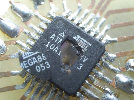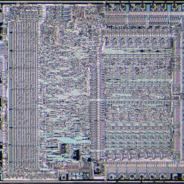
Unfortunately [manekinen] wrecked a couple of AVRs during his tinkering. Not letting this get him down he decided to blow them up to see what would happen. In exchange for their precious magic smoke the AVRs revealed a good portion of their silicon die.
While the details are a little sparse it seems like he hooked them up to a high (and possibly reverse) source to blow open the chips casing. From the pictures it looks like he was able to reveal some of the flash or SRAM (the big multi colored rectangles) and what could possibly be the power supply. Be sure to checkout the videos after the break for some silicon carnage.
[youtube= http://www.youtube.com/watch?v=4YEL7Jx26Wk&feature=related&w=470]


Rest in pieces…
Interesting, I had a similar experience when incorrectly wiring a stepper motor to an ULN2803A OCTAL DARLINGTON! Fry!!!!
The chip casing properly flys, i would love to see this in superslow mo.
Had this happen to me once (though i cannot remember what i was tinkering with at the time)
Heard a loud snap and a small black bit landed near me, took me a minute to work out where it took off from!
very nice explosions, actually. :)
Could be the solder bridges…
You should see big industrial gear that this happens to.
Think large smouldering holes in PCBs and dented sheet metal.
Try putting a windowed EPROM into the programmer the wrong way round. You get a nice light show of tiny blue flashes but sadly a non-functional chip afterwards.
Back in the 90’s I had an internship at a semiconductor company, AMD, where I worked in a device debug group.
One technique for troubleshooting bad packaged die was to “decap” them by eating the plastic case away with a couple drops of nitric acid on top of the device. (Under a vent hood. Wearing gloves and goggles.)
The die would be exposed with the lead wires still attached. After having the acid washed off and being dried, the device would be put on a test rig inside a dark box with a thermal camera focused on the exposed die. When power was applied to the device, sometimes hot spots would show up at flaws.
A guy I knew in a mil lab over 20 years ago ragularly blew up defective Z80’s by connecting each mains (240V here) rail to each Z80 pin line.
Nothing ever works the same after you let the blue smoke out. Wish I could get that stuff in some sort of recharging can.
I wonder what that second explotion was from in the Mega32 (first) video.
Seeing bits of hardware blown up kinda makes me shiver >.<
Please! send me the code to do that!!
Didn’t know that the AVRs had the HCF instruction so dearly beloved of the 6809…
http://en.wikipedia.org/wiki/Halt_and_Catch_Fire
now what did those little bits ever do to deserve that!
It isn’t entirely clear but many of these could probably have been fixed. Bad fuse settings can be undone. Even when part of the ic is dead the rest usually still works.
Avrs seem to be very resiliant. I have nuked a couple with backwards supply lines etc. They smoked but still work
I hope he learns to solder a little better too.
electronics run on smoke. the electricity is only there to hold it in. Once you let it out it doesnt work anymore
Another great tool for popping the IC package is a $3 electric fly swatter. Used one with a resistor as a low tech method of apply a simulated esd event to a chip as part of and FA debug. After I got the needed results applied it full force to the QFN parts and they would jump and blow the package apart. The simple joys in life. Under the microscope the silicon looked like a cd placed in the microwave.
@Peter
Ever get to see one running, decapped in a sem? That is awesome. I love my job. :)
@Jaspel
Afraid not. That sounds really neat!
I’ve heard that you can probe the running circuit with a SEM, getting voltage levels without physical contact. Is that true? That would be interesting for reverse engineering work.
The two debug groups I worked in were sort of last-ditch low-effort trouble-shooting teams.
Most of our work was just blindly rerunning the original simulation and looking for obvious failures. Or working to shepherd devices through wafer sort.
But for older devices, it was a real pain. The designers had moved on. We didn’t even have a valid license for the EDA software in some cases. Some of the EDA vendors had gone under. The simulations had to run on Sun OS boxes with the date set back.
The big push at the time, I vaguely recall, was for “Design for Test” and JTAG. I missed out on that because I ran off to join the Linux circus in 2000. I haven’t worked in the Semiconductor industry since…
Luckily I have a stack-overflow check in my main loop. Doesn’t work against infinite recursion though.
@ Peter
With proper hardware, I don’t see why not. Our EDX is running win3.1 with no support. As an independent bottom feeder, we won’t upgrade until it dies.
damn good reason to current limit during devtime. Good job ! p.s YUCK to atmels, Viva la PIC ;)