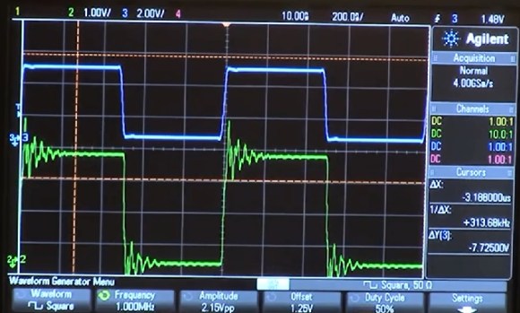
In high speed digital circuits, fast doesn’t necessarily mean “high clock rate”. [Jack Ganssle] does an excellent job at explaining how the transition time of signals in high speed digital circuits is just as important as the speed of the signal itself. When the transition time is large, around 20 nanoseconds, everything is fine. But when you cut it down to just a few nanoseconds, things change. Often you will get a ringing effect caused by impedance mismatch.
As the signal travels down the trace from the driver and hits the receiver, some of the signal will get reflected back toward the driver if the impedance, which is just resistance with a frequency component, does not exactly match. The reflected signal then heads back to the driver where the impedance mismatch will cause another reflection. It goes back and forth, creating the ‘ringing’ you see on the scope.
[Jack Ganssle] goes on to explain how a simple resistor network can help to match the impedance and how these should be used in circuits with fast transition times, especially where you will be taking readings with a scope. As the scope probe itself can introduce impedance and cause the ringing.
In case you didn’t pick up on it, [Jack Ganssle] also happens to be one of the judges for The Hackaday Prize.


“impedance, which is just resistance with a frequency component” while technically correct in other contexts, is highly misleading in this context. Characteristic impedance of transmission lines is not the same thing as impedance in general.
As an example, putting an ohmmeter on a 50 ohm transmission line will not give you a reading of 50 ohms.
An Ohm meter lacks the ability to measure the frequency component as it only measures DC resistance, this example is somewhat self-defeating in that aspect.
actually it would, if the transmission line was infinitely long
The “50 ohms” is only the magnitude as it is a complex number with a real (resistive) and imaginary component (could be inductive or capacitive).
http://hyperphysics.phy-astr.gsu.edu/hbase/electric/impcom.html
No, transmission lines are (close to) purely resistive.
It is just that the ones that you worry about in digital signals are the “very short transmission line”.
http://home.sandiego.edu/~ekim/e194rfs01/tlsmthek.pdf
” Waves and Impedances on Transmission Lines”
page 13:
> A very short transmission line terminated with a open is capacitive and has negative reactance Z = 1/jωC, and in fact this entire hemisphere of the Γ plot is capacitive (negative reactance).
> A very short transmission line terminated with a short is inductive and
has positive reactance Z = jωL, and in fact the entire upper hemisphere of the Γ plot is inductive (positive reactance).
^aren’t
Characteristic impedance and impedance are not the same thing. As far as I can see characteristic impedance was not mentioned. I do have to agree though that “impedance, which is just resistance with a frequency component” is a pretty bad thing to say, at the very least you should replace “frequency” with “phase”.
How is phase more accurate than frequency, considering frequency part of the equation and phase shift has no affect on impedance
“impedance, which is just resistance with a frequency component” << incorrect
“impedance, which is just resistance with a phase component” << correct
The first statement is not true, the second statement is true.
http://cds.linear.com/docs/en/application-note/an47fa.pdf
they solved this problem on cpus and busses by coiling the lines
the squiggly lines are there to make all the lines the same length, still need to have proper termination when the rise time is short compared to the wire length
3rd person to get this wrong in the past week.
They have nothing to do with signal quality. That only deal with flight time in timing constraints. They are there to make sure that one group of signals has a certain delay vs another one which is typically a clock to satisfy a set up time requirement.
I would have said that they have everything to do with signal quality… The point is for the noise on the +ve diff signal to arrive at the same time as the -ve to the subtractor amp- cancels out any noise…
That would only applies when you are matching skews on a differential pair that takes out common mode noise. If there is differential noise e.g. when one or both of the pairs hits a impedance discontinuity/reflection or mismatch, that cancellation would not work.
Most of the time what you see on “cpus and busses by coiling the lines” are single ended signals (usually data lines or address lines against vs clock). You can spot differential line very easily as you have a pair of lines that are very close and follow each the other and far apart from other signals.
Common mode noise = external noise that is seen by both signals in a diff pair.
A differential pair would have 2 signals that are 180 degrees out of phase. So if one of them going on a rising edge, the other would go on a negative edge. Now if these signals are not terminate correctly, then on of them would see an overshoot while the other sees an undershoot. When you subtract that, you get 2X the amount of noise as the noise are also going in opposite direction.
Only when both signals overshoots or undershoot at exactly the same way would you cancel them out by subtraction which is impossible by definition in a differential pair..
Interesting! certainly makes sense… Does anyone have an example of a single signal where ‘coiling’ (terrible description) is used – seems like ridiculous timing constraints if a few extra mm can make the difference?
You would need to worry about track skews when they take up a big chunk of your timing window.
http://blog.optimumdesign.com/ddr-memory-layout-design-rules-factors-considerations
Clock line in DDR is differential pair and data line etc are single ended. They show you both types.
the PCB delays is adjusted for:
Clock-to-Address/Command Group:
Clock-to-Strobes Group (CLK/STB):
Strobe-to-Data Group (STB/Data):
Electronics is the art of signal conditioning. That is all for now.
For those that want to read more on this subject in general, and any EE/CE in general:
Right the First Time by Lee Ritchey (now a free pdf book) does the best job of intuitively explaining impedance mismatches and all other phenomena happening with fast digital boards.
Get this book right now. In my opinion it is more directly usable and useful than the much-praised Howard johnson’s “Black magic handbook”
Even all you arduino-tards out there need to read it. Everything anybody does now is affected by fast edge rates.
“arduino-tards”???? That stings bro! You could lose your hackaday privileges for slinging around some saucy slurs like that!!!
Seriously though, from the article: ” the impedance, which is just resistance with a frequency component” <—– this is one of the most inadequate explanations I have ever seen.
It is a lost cause for that group. It is not like they would get away from poking piece of wires into their ardurinos or use breadboard and loose wires for their circuits. The last thing they would learn using proper PCB controlled impedance, adding decoupling cap, making sure there is a good return path for their signal and adding proper terminations for the transmission lines.
I quickly skim through the “material” and found it very lacking. What is important is the rise and fall time of the chip driving the signal not the actual frequency. That rise/fall time tells you how long a track is before you start seeing enough of the transmission effects and have to deploy a terminator of some kind. If the track is short relative to the rise/fall time, then it would only see a small step of the signal each time before the wave front get reflected back a few time and dissipate.
The frequency is only how often that transition happens per second. You can have an insanely fast chip that switches 10 times a second, but produces bad signals every time it switches.
wow, its like you copy pasted captions from the video …
To the amateur engineer, I think this video explains a very complex process in understandable terms. Everyone criticizing the content is looking at it from a much higher level field than what this video is aimed at.
Did anyone else notice that his example of the impenetrability of Maxwell’s equations was doubly effective? He put up a “deliberately incorrect” equation, then got the verbal correction wrong too!
(He should have said: Change the B on the right to an E, and add mu J to the right too. The wrong equation he shows is a lot closer to the “Ampere’s law” one than the “Faraday’s” one. If he’s going Faraday, he should also have swapped the mu.epsilon multiplier for a minus one!).
Also yeah – it’s not just the driver and load impedance matches that matter, although that correction is often all that’s done in old/slow (arduino grade) logic like he obviously deals professionally with.
But that’s what happens when you try to use single ended, traces or busses without a ground plane. Even “matching” the ends of the trace does you little good, if the trace hasn’t got a single characteristic impedance all the way along its length to start with. (and without either differential wiring or a ground plane with consideration given to the return current path, it sorta can’t. Anyone remember 80-conductor IDE cables? They were so the current loops formed from having a single earth return wire on the 40-pin cables didn’t make the ribbon into a stack of overlapping, one turn transformer windings! )
If your cable don’t have a close by ground, “nature will find a way” and use the closest signal(s) for its return path. You would see cross talks between signals cause by inductive coupling when the signals are much closer together to each other than ground. Yes even where there is a ground plane further away.
In fact the later ATA specs have to deal with the not having close enough grounds signal arrangement when they move towards Ultra DMA. They have a section on signal integrity and simulations. (SCSI on the other hand starts off with 1:1 signal/ground arrangement ignoring Apple’s use of 25 pin SCSI at one point in time.)
>This combination of factors results in the impedance of the conductors in the center of the set of data lines rising from 110 to 150 Ω (measured when a single line is asserted or negated) to an almost purely inductive 300 to 600 Ω when all lines are asserted or negated simultaneously in the same direction. Measured impedance varies with data pattern, edge rate, cable length, loading, and distance from chassis ground.
Yikes!
The title is wrong, it should be “analogue design for high speed digital signals” not “high speed digital design”. It is also proof that there is no such thing as a digital design engineer, if you can’t do analogue you can’t do digital either. :)