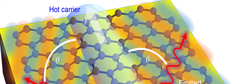
When a supersonic aircraft goes faster than the speed of sound, it produces a shockwave or sonic boom. MIT researchers have found a similar optical effect in graphene that causes an optical boom and could provide a new way to convert electricity into light.
The light emission occurs due to two odd properties of graphene: first, light gets trapped on the surface of graphene, effectively slowing it down. In addition, electrons pass through at very high speeds. Interestingly, the speeds are nearly the same–that is, electrons and trapped light travel at almost the same speed. The researchers found a way to make the electrons move faster than the speed of light (in the graphene) and thus created Cerenkov emissions. Because of the structure of graphene, the resulting light is intense and tightly focused.
The researchers speculate that this technique could be important in building graphene-based optical chips. We’ve talked about mixed graphene and semiconductor chips before. Graphene is pretty exotic stuff. It can even fold itself.


Won’t believe it until I see it.
2030 flatscreen TVs.
This is science, not a bible class debate, there is no believe or not believe.
Anyway by 2030 you will have probably lost your one good eye in some sort of back yard science misadventure and will not be able to see anything.
You apparently aren’t aware of the over embellishment and rampant false claims present in scientific journals then, or this popular published paper. https://scholarlyoa.com/2014/11/20/bogus-journal-accepts-profanity-laced-anti-spam-paper/
Have fun with your religion, I know for a fact whole ionic colloid copper chloride supercapacitors do not exhibit over 5000 farads per gram capacitance and that is what opened my eyes.
Whatever, I’m also pretty sure not having a sense of humor is statistically correlated with mental illness and having a shorter lifespan. So I wish you good luck with that, and I hope you make the most of the time you have left. Good luck getting a gun license too. LOL
Correlation is not causation
PurpleTurd, your name is appropriate—you could have also just gone with Turd
Nature has a good reputation. That being said – some papers are clearly stunts that hype the potential of new technology. (That Kilocore paper is definitely a stunt. Single Thread Performance is king in High Performance Computing.)
T
L
;
D
R
Yeah…. and cold fusion is “science” as well as perpetual motion….
Excess heat with palladium in the nuclear density range is very real.
The fraudster in that case were the MIT people, and billion-dollars funded hot fusion scientist.
It does make sense when you think about it. And if you read about it you’ll learn that it is fact.
I’m sure it seems easy to mock others for something you don’t agree with it or understand, but it takes far more courage to admit the truth to yourself and others. It’s hard to win an argument of truth with an intelligent and reasonable person, but near impossible to a person of ignorance, and doubt. Which do you want to be? If courageous and reasonable, then seek out Him who is. See if he is for yourself.
Laser guns. Heck yeah.
(This is my latest effort, although it’s just a diode laser. https://www.youtube.com/watch?v=EsPn-P4xzkc I’m going to sell a few and then open-source the design, same as last year)
Laser guns? Heck no… at least not against people. Against things, there already are systems being tested/used…
Open lasers in 3D printers always scare me. I hope you are using protection glasses?
Could be something useful eventually
Describes literally every application I’ve seen for graphene. All hype, no delivery.
That is just about the size of it.
Seems legit to me.
It’s just the conservation of energy in a different medium. The lattice structure of graphene is causing and accurate averaging of electron flow (from photonic absorption or eV) by creating polarized (electron repelling) nodal points where the flow is greater. This in turn allows a higher photonic re-absorption until the point of saturation and then you have spontaneous photonic emission in accordance with the conservation of energy.
I wonder if the light output is highly polarized in thinner graphene structures.
This could give us more efficient power LASERs.
Some things take time – there’s a difference between creating a proof-of-concept thingy on a <1mm^2 graphene using crude methods (Scotch tape) and incorporating that in a device that can be manufactured.
Compare to semiconductors – point contact diodes (probing a crystal until a semiconducting region was found) and transistors (ditto). It took time from the proof-of-concept stage to the manufacturing stage and even then the early devices were crude and not that exciting performance wise. But while a crude semiconductor device was possible to "mass" manufacture the same isn't true of graphene devices – to be useful it have to be integrated in modern ULSI chips. And that is pretty complex, just reliably laying down a single layer of carbon atoms is hard, avoiding the carbon contaminating the silicon is hard, forming reliable contacts with the carbon is hard, compensating between lattice mismatches is hard etc.
If you want a reasonable comparison just look at III-V semiconductor integration in a modern process flow. Then realize that III-V is in comparison a solved problem, it is possible to lay down e.g. GaAs on silicon wafers and make working devices and have been for a long time. But it isn't (yet) reliable enough to replace silicon based semiconductors even though the performance difference can be huge…
Link to the paper for those that want to read lots of formulae:
http://www.nature.com/ncomms/2016/160613/ncomms11880/full/ncomms11880.html#abstract
Am I the only one that took HaD’s summary of the SciTech summary to mean that the researches used electricity to release stored photons via Cerenkov emissions?
Cause that’s not what’s happening.
I’m guessing the electrons are emiiting photons instead of going faster than light when energy is applied to them.
or after reading the wikipedia article on cherenkov radiation, I see I could be completely wrong.
your not wrong at all. These things are black boxes and we can only see or measure what escapes out of the black box.
Electrons have fixed (granular) levels of kinetic energy rather than variable levels so they emit photons when they need to dissipate energy to achieve a lower energy state and on the other hand they can equally absorb a photon of energy when raising one state in kinetic energy. This happens all the time and only some portion of this energy escapes the medium (normally).
I think the difference with graphene is that it reduces this internal emission / re-absorption so that it has a much higher energy saturation point where the energy emission from the medium is spontaneous.
You are perhaps thinking of electrons bound to atoms? Free electrons, like in a CRT take on whatever energy they get from acceleration by the electric field. Metals (and apparently graphene) have free electrons. That is why you can shake them about in an antenna to get EM radiation and why antennas are not made of plastic.
@[TheRegnirps]
All true but that is not the attribute of electron flow that is responsible for this property.
Free electron flow is chaotic. This principle relies on ordered electron flow.
Faster than light in the media. It is what causes the blue glow from reactors in water. Energy is dumped as light when something enters the water at FTL (in water). The speed of light in a medium is the ratio of the permittivity to permeability. In vacuum it is highest.
I understood the Cerenkov emission, the wording just made it sound (to me) as if electricity was amplifying / triggering a release of stored photons. I was just seeing if I was the only one reading the summary wrong.
The research paper and complementary MIT press release clarified my reading error.
Graphene Clothes will = http://www.criticalcommons.org/Members/michacardenas/clips/ghost-in-the-shell-falling-fade/view
Seems to me, going by the synopsis, that this could be a continuous tunable light source with many many applications. And, close to if not, coherent. If efficiency is high, really amazing.
Finally I’ll be able to stop lighting my house with nuclear waste in as bucket of water!
If you had something with enough activity to give off visible Chervenkov radiation in a bucket of water, the water would boil off fairly quickly, you’d have to constantly top it off…maybe air ionization would give off some light as well? :D
I don’t recall any heat problems in research reactors, but the pools are pretty deep and big enough to stop nearly all forms of radiation coming from the reactor. Must have been passive cooling.
Wow that’s great!
What is the orderable part number for this part?
What? No part number?
Was my attention just “Hacked”?
Your short sightedness is sad.
If tugboats were bigger, they could be the boats that other boats tug.
..or perhaps Boaty Mac Boatface… ?
lol
Turtles … all the way down.
I would like to buy some graphene. Everyone should be buying stock in this. As soon as we can 3D print graphene products, global warming will end, and every country’s borders will be safe and secure. Graphene is the love-child of Avogadro and Tesla.