A while ago, [Marco] mounted a powerful laser diode to a CNC machine in an attempt to etch copper clad board and create a few PCBs. The results weren’t that great, but the technique was promising. In a new experiment, [Marco] purchased a very cheap laser engraver kit from China, and now this technique looks like it might be a winner.
[Marco] sourced his laser engraver from Banggood, and it’s pretty much exactly what you would expect for a CNC machine that costs under $200. The frame is aluminum extrusion, the motors are off-the-shelf steppers, the electronics are just Pololu-like drivers, and the software is somewhere between abysmal and terrible. Nevertheless, this machine can cut wood, leather, fabric, and can remove spray paint with a big blue laser diode.
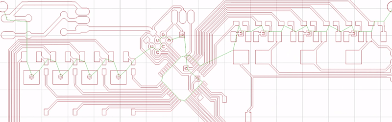
To create his PCBs, [Marco] is first cleaning a piece of copper clad board, coating it with spray paint, then blasting it with a laser. The preferred software for this is LaserWeb, and the results are pretty good for a cheap machine.
There are a few extra steps to creating the PCB once the board has been coated with paint and blasted with a laser. This process still requires etching in either ferric chloride or some other mess of acid, but the results are good. So good, in fact, that [Marco] is experimenting with copper foil and Kapton to create flexible circuit boards. You can check out the video of these experiments below.
Thanks [ganzuul] for the tip.


I believe that laser cutting shops don’t like to cut copper, as their operators get flash burns from the process. I think it was copper, anyway.
He is not cutting copper but the etchresist on top of the copper.
He is not cutting copper but the etchresist on top of the copper.
Still, once the resist is burned through, laser beam hits the metallic copper surface and scatters.
I have been doing this for more than a year, my results are that what you want to do is use the laser at a slight angle. Otherwise a significant part of the beam may go back into the diode, and damage it. (This has only happened when I was trying to etch the board with ferrochloride paste on it, the paste melted and acted as a mirror, but still).
Ah, my bad. I misunderstood the process.
Can’t see what’s wrong with tracing paper photomasks made on a laser printer, and Kinsten pre-sensitized PCB? Works great for me!
Copper has some of the worst reflection issues of any material you are likely to try laser cutting, short of silver or gold. If you have the proper enclosure in place on your laser, and don’t try to pick up the workpiece bare-handed after cutting it (it’s going to be extremely hot), the operators aren’t in any particular danger. The laser optics are another matter; it’s very easy to blow out the lens from reflections.
I did cut a piece of 1 mm copper once using a 4 kW Amada Gemini. The feed rate was about as slow as cutting 6 mm of aluminum or 12 mm steel.
I doubt that. Just look at what happens when you try to cut something and the bed height is a few mm off from putting the target at the same level as the laser is focused. You are suggesting that a reflection off of a piece of copper is going to cause a burn skin from some number of feet away?
Maybe, just maybe there might be a reflection that could damage an operator’s unprotected eyes. A proper pair of glasses chosen to filter the correct wavelength of light aught to prevent that just fine.
I wonder what type of laser is used….specs?????
The only bad that about cutting copper is the fact that it takes fine tuning and you have to run high power at a slow rate with high pressure, pretty much its expensive to cut. So if operators are getting flash burns its either because they are pushing the machine because stupid or their boss is telling them to speed it up because stupid.
I recently got one of those kits too from banggood, Eleks A3 2500mW for €170 shipped. Assembly went well, hardware works fine, but the software Eleks provides is downright horrible. SVG doesn’t import correctly for starters, and it will send malformed GCODE to the machine and ignore its returned errors if your Language/Locate Settings is set to have a colon (,) as decimal seperator. Took me some time to find that one. The other supported software, benbox, can’t seem to control the laser on my “Mana SE” controller. I have not had the time to look at LaserWeb yet. Also the laser and controller both support PWM, but no PC software seems to support it. I have not had a lot of time to play with it yet, but i bet i’ll probably end up writing software myself.
laser etching pcb’s was also of interest to me as i was hoping to get rid of the messy FeCl3 etching, but cutting that copper would require quite a bit more power i understand.
i meant comma, not colon : “,”. It obviously uses the Locale Settings to do float to string while GCODE always expects a period as decimal seperator.
A laser is pretty much the worst thing you can use to cut copper, which is reflective and conducts heat well. You’d be better off with a micro mill, really.
This is only true for very thick copper or if speaking of CO2 or very low power diode and fiber lasers. Laser cutting copper with KW class lasers is done as a matter of routine every day all over the world. Copper cutting with a blue wavelength should be no problem at all since the absorptive properties of copper in that wavelength range are similar to steel and CO2. Whoever harnesses Blue into a KW Class high brightness laser source will revolutionize industrial metal cutting.
These little blue engravers are a big step in bringing that wavelength to the CNC world and I am impressed with what I see so far.
PCB laser direct etching can be done with a trippled Nd:YAG laser. LPKF sells a prototype manufacturing machine. But as said earlier: Holes, especially plated vias are the real problem.
Isn’t copper pretty much the worst thing you can cut?
As noted above, a kilowatt range YAG or visible light laser won’t have too much trouble with copper. If you’re assuming it’s a CO2 laser, the worst material I ever encountered myself was ordinary window glass, a quarter inch thick. The trouble was that it was way too easy to shatter. I could get the laser to cut 1/8″ thick window glass, but the thicker stuff was very difficult.
Gold is supposedly nearly uncuttable with a CO2 laser, though I don’t have firsthand experience with that. And there are some materials that fall into the category of “No. Just no.” Magnesium, for example, is something you could probably cut if you used a nitrogen assist and a large enough nozzle – but I don’t want to be in the same room if things go wrong. Beryllium-copper alloys are another on that list. The fumes it would release would make heavy metal poisoning look like the common cold.
You would need a much bigger CO2 laser with air assist to cut copper and even then it would suck because of the very good heat conductivity of the copper (the laser melts the metal and the compressed air blows it out of the cut). Small semiconductor lasers like your diode (likely originally meant for Bluray burners) are totally hopeless for such job.
CO2 is a bad choice for copper… Q-switched DPSS YAG is a much better choice, but it’s obviously more expensive and has a much more complicated optics assembly.
He is just burning paint, acting as an etch resist. This is of course much easier compared to lasering the copper directly.
That’s basically how PCBs were made at Texas A&M. It was able to “print” down to SOIC pitch very easily. The via plating, though, left much to be desired. Gets pretty exciting when a 330uF capacitor charged to 270V arcs over a blown via…
Definitely look at LaserWeb! One thing I noticed about the 2500mw I bought (https://www.aliexpress.com/item/DIY-mini-2000mw-2w-large-engrave-carve-machine-350-500-laser-engraving-carving-machine-laser-printer/32611833032.html) is that they wouldn’t give an updated GRBL source (only pre-compiled and old). Found out they made their own board and swapped around the outputs, so I just remapped it in GRBL and uploaded it. Had to do this to get it working with LaserWeb.
so i did take a look, the standard firmware for the Arduino Nano that Eleks provides seems to be grbl 0.9, but laserweb needs >1.1d. I verified that the step and dir pins are the same as the default config, and the laser PWM is on PB3 (D11), that all seems to be in line with the default grbl config. So i tried the stock 1.1f grbl firmware and the machine moves but does not report position. So i had the change $10 to 0 or 2. Also set $32=1 to enable laser mode (so the machine doesn’t stop on changing S). It is now reporting position correctly, but the laser is not coming on with M3 or M4 with any S value .. It also goes into alarm mode after boot because homing is disabled by default (don’t have any reference switches anyway). So I have to issue a $X to clear the alarm state after boot. I also need to find the correct steps/mm settings again, since the EEPROM was overwritten with new values that are not correct. I tried compiling the firmware (to disable alarm state on boot) on raspbian but the resulting hex file just gives me a “error 7” (eeprom read failed) and then stops responding. I have not verified this toolchain, so i might try again on windows using the arduino IDE. So I still need to get the laser working.
ok, so it’s 80 steps/mm for these “Eleks Lasers” ($100, $101), and the laser is working fine now too after setting the test power > 0% in laserweb4. The stock firmware grbl v1.1f is running fine on the Eleks Mana SE board. This does seem like the way to go, the only thing that might be handy is some tools to quickly create lines and text. Oh, and a running time estimate.
I think that’s what I came up with too, 80 steps/mm. It’s close enough.
What is the accuracy of the laser? Can it do like 10/10 mill traces?
That depends on how much time you spend focusing it, but in general 10/10 is realistic, 10/6 is feasible if you spend a lot of time playing with it and have a good mill to start with. For smaller traces, the etchant will go under the paint and you may get cut traces, so don’t.
Seems ok for quick turnaround pcbs.
Now i know what to ask santa ;)
The problem isn’t the accuracy, it’s the spot size.
The very expensive ($5K) laser at our hackerspace has a spot size of about 0.02″, which is about 1/2mm.
The positioning accuracy is very good, about .02mm, but when I tally up the trace width and minimum line thickness (one etched 1/2mm line each side of a trace, plus trace width) I found that you can’t run a trace between two pads.
I’d love to use this as a technique, but it can only work for large components.
If you want to try it you don’t need etch resist – just spray some black paint on the PCB and dry it in an oven for an hour or so. Run the etch twice – once to remove the paint, and once to remove the splatter from the 1st run.
Then wipe gently with alcohol to remove any remaining splatter, etch, and wipe with Acetone to remove the paint.
The beam coming out of the laser may be too wide, but would it be possible to have a narrower diameter mask mounted to the laser assembly?
On an unrelated note, how about giving the copper surface an oxide coating with some salt water first so it wasn’t reflective. That would presumably avoid the problem of the beam reflecting back into the laser assembly.
Perhaps any machine like this one should have a big red toggle switch mounted right on the laser head. So that when its off, you can be sure its off.
On the bearing / belt guide combo. there may be some unintentional wear because unless the bearing contact and belt contact radii are the same, somewhere there has to be some slippage.
Looks like good value though.
The one I sell has a tilt switch, it’ll only fire if aimed downwards and moving relatively slowly. Safety concerns really, doesn’t do much for repeatability. I find that a 3d printer with kevlar belts will work well, though.
The biggest problem is still the same: You can not make plated vias.
Yeah. We had a micromill at university, it didn’t get used much because of that. The plating machine is still insanely expensive.
People did this years ago, and managed double sided solder masks by engraving a second time after etching.
Plating takes drilling prior to etching, simple low-resistance chemical coatings (often toxic), and a CV CC DC power source.
But for under $60 I can get 4 layer @10 pcs with better accuracy.
Most people’s time is valuable after all.
Or a simple non-isolated wire, soldered on both sides, for hackers on a budget. It puts “not” in “rapid prototyping”, but hey, at least you are not waiting for PCBs to arrive.
So? Just don’t design with plated vias.
People got by designing electronic devices without plated vias for decades. Does everything you do as a hobbyist have to match the industry’s cutting edge? Consider it a design challenge. Show that you can create a good board even with fewer features available to you than what the board houses have.
I did such a board once: 8051 circuit and several 100 vias with hand soldered wire in the 90ies. It was quite a PITA and I broke some 0,5mm drill bits while drilling the board. I noticed only after finishing the layout, that the default via was quite small :-(
I am really happy about the progress, electronics has made in the mean time. But now my focus is on optimizing the circuit and function with modern SMD components and technologies and not on doing it with outdated technology. Luckily there are affordable real PCBs (with plated vias, solder mask and fine lines) from places like OSHpark or DirtyPCB.
I also can’t understand this “retro computing” hype or “lets do something with oldstyle TTL, 6502, Z80 or nixies or other tubes”. I had a C64 and it was great for it’s time, but times are changing. When I got my 486-33 PC I soon after sold the C64 stuff.
Totally agree. For proof of concept for ‘home hackers’ though this is a nice alternative. Waiting a week or so to prove a circuit out can be frustrating. I would love something like this in my home lab
Agree on avoiding vias (and double-sided) for home fabrication. I prefer to use a 0 ohm 1206/1210 resistor instead to cross tracks.
I don’t know any rivets, that can realize 0,3mm vias, and you have to solder them, if you want any durability of the board and not only a pile of intermittent connections. Rivets are just not compatible with modern PCB line/space design rules.
Has anyone tried this process on a Co2 Laser Cutter? I have been thinking of purchasing a cheap Chinese 40w Co2 Laser Cutter from that famous site where you bid on some things but mostly just click buy it now.
I’m wondering if the Co2 Laser can blast away the spray paint “resist” with the same effectiveness as this machine.
Ive used a 60W CO2 laser to burn away paint. works great. Problem in this case is the copper underneath. Copper (as I was told) is highly reflective in the infrared range the typical CO2 lasers output in and reflections can damage / burn the lens and release dangerous chemicals in the process.
Working with a slight angle might work to take care of reflections but I didn’t dare to try yet. The machine was damn expensive.
WIth 40W it will certainly vaporize spray paint. You will need to turn the power down though, as the bare copper below the paint will reflect the light back into your source. A CO2 tube probably won’t care, but the lens likely will. In my experience, Chinese CO2 tubes are fine and work just as long as western brand name ones.
I have one of these cheap Chinese laser cutter. Though, I have been thinking of attaching a low powered UV laser to it, and simply expose photo-resist with it instead. As the driver board I have installed has multiple laser outputs. So no reason to not try. The laser isn’t expensive, and building a small driver board for it is just an op amp and a few resistors in my case. As a 5mW 405nm laser should be plenty to expose photo-resist. Worst case I need two or three passes. But better then wait around a week or two for a prototype to get shipped in from another part of the world.
But well, one could most probably use the 40W laser tube as well at a decently low power and simply use spray paint or similar as an etching barrier instead.
I don’t recommend that. I’ve tried that 2 years ago, described it here:
http://www.eevblog.com/forum/beginners/practical-proscon-of-laser-vs-milling-of-pcb's/msg766269/#msg766269
Too slow, low quality, some etch-resistant film still left after vaporizing. I’ve used 1W laser, maybe something like 2-3W or 40W CO2 would be better, but it opens other cans of worms, either unsafe (I consider 445nm power lasers the most dangerous things in my lab) or damages ZnSe lens. Copper not only reflects laser brilliantly, but also absorbs the heat, therefore making the paint evaporation task much harder.
I want to try the UV exposure method (see http://www.diyouware.com/node/161) with much lower power laser, on a 3D printer (therefore faster than CNC). Should be better, but it adds more wet processes which I’m not a fan of.
Has anyone tried using a laser to expose photosensitive boards?
Yes, not really the right wavelength. But you can take a UV Lamp and focus it.
What would the advantage be against using “any” paint and burning it away?
fibre optic laser technology is able to cut brass, copper and bronze up to 10mm thick without a problem. There is a laser out there to cut it lol.
If it were me, I would just use the Banggood laser engraver with a small dremel type rotary tool rigged to it (in place of the laser) and simply remove the copper mechanically. Sure, the cheap features of this unit would not really support much in the way of milling but, removing that soft, thin layer of copper from a board should be within its abilities I would think. I am sure someone has already done this somewhere.
Without a proper Z axis, it goes all over the place. I tried :)
Mechanical depth stop.
Actually, you need to use 3D leveling as even minor variations on depth will undercut or overcut the pcb. It just requires an allegator clip to the board and another to drill bit. Let it problem surface in a grid and then adjust GRBL to depth map. Voila!
Few guesses: You did not show any actual circuit board, did not even show a close up of the etched board so that we can asses the quality. Plus, maybe they could not stand how messy everything in your video was :) No offense.
Thanks!
I’ve directly laser ablated the copper on a copper clad boards using a 40w Fiber laser, worked just fine, I’ll get a picture tonight.
It’s incredible how hard people try to do something with a laser (buzzword!) involved, instead of just using a simple desktop milling machine. Why going easy, if there’s also a complicated way, right?
better resolution?
I saw the guy with the Swiss accent do it with one of those 3040 milling machines, and the process looked terribly complicated.
I have used both, and found that the laser is much easier and can deliver finer traces and spacing.
I’m surprised no one has mentioned T2 laser (t2laser.org) as an alternative to benbox or laserweb. It’s pretty good sfotware, is updated quite regularly, and the developer responds personally to support requests. It’s also not expensive, around $40 if I remember right. I’ve been using it on my BG laser engraver for about a year now and have been quite happy.
oof, holy PPE, batman! Why aren’t you using gloves? Acetone, Ferric Chloride, as well as all the byproducts (like Copper II chloride)… Why expose yourself to those if you don’t need to?
hello,
can anyone tell me what machine is he using for this process ? or is it custom made ?
thank you in advance.