Designing combinatorial digital circuits seems like it should be easy. After all, you can do everything you want with just AND, OR, and NOT gates. Bonus points if you have an XOR gate, but you can build everything you need for combinatorial logic with just those three components. If all you want to do is design something to turn on the light when the ignition is on AND door 1 is open OR door 2 is open, you won’t have any problems. However, for more complex scenarios, how we do things has changed several times.
In the old days, you’d just design the tubes or transistor circuits you needed to develop your logic. If you were wiring up everything by hand anyway, you might as well. But then came modules like printed circuit boards. There was a certain economy to having cards that had, say, two NOR gates on a card. Then, you needed to convert all your logic to use NOR gates (or NAND gates, if that’s what you had).
Small-scale ICs changed that. It was easy to put a mix of gates on a card, although there was still some slight advantage to having cards full of the same kind of gate. Then came logic devices, which would eventually become FPGAs. They tend to have many of one kind of “cell” with plenty of logic gates on board, but not necessarily the ones you need. However, by that time, you could just tell a computer program what you wanted, and it would do the heavy lifting. That was a luxury early designers didn’t have.
Basis
How can you do everything with a NOR gate? Easy if you don’t mind spending gates. Obviously, if I need a NOR gate, I’m done. If I need an OR gate, I just feed the output of a NOR gate to all the pins of another NOR gate. The output of the second gate will be the OR of the first gate’s inputs.
DeMorgan’s theorem tells us that if NOT(A OR B) is the same as (NOT A) AND (NOT B). It is!
| A | B | NOT A | NOT B | NOT(A OR B) | (NOT A) AND (NOT B) |
| 0 | 0 | 1 | 1 | 1 | 1 |
| 0 | 1 | 1 | 0 | 0 | 0 |
| 1 | 0 | 0 | 1 | 0 | 0 |
| 1 | 1 | 0 | 0 | 0 | 0 |
So you can create a NOT gate with a NOR gate (or a NAND gate) and an AND/NAND gate by mixing up NOR and NOT gates. Conversely, you can create OR/NOR gates by mixing up NAND and NOT gates. So, either way, you are covered.
The only problem is figuring out how to express any arbitrary expression as a bunch of NOR or NAND gates. A common way to do this is to have a “product of sums” or “sum of products” arrangement. In this context, a product is an AND gate, and a sum is an OR gate. This also works with things where you use diodes and wired AND logic, such as those you find in a programmable logic array or open collector arrangements. Think about it. A bunch of open collector outputs tied to a pull up resistor acts like a giant AND gate. Any low input causes a low output.
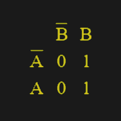
Suppose you wanted to determine whether a two-bit binary number is odd or even. Yes, yes, there is an easy way to do that, but assume you don’t know that yet. Let’s assume the most significant bit is A and the least significant is B. Further, we’ll use the notation A’ for NOT(A). AB is A AND B, while A+B is A OR B. The two odd values are 01 and 11, so we can set up another logical Y that is true when we have one of those OR the other:
Y=A'B + AB
Troubleshooting
This works, of course. But if you are adept at troubleshooting digital logic, you might notice something — again, assuming that you don’t already know the answer to this problem. The output, Y, doesn’t really depend on A at all because we have A’B or AB together. So just intuitively, we know the real answer is Y=B. No gates are needed at all!
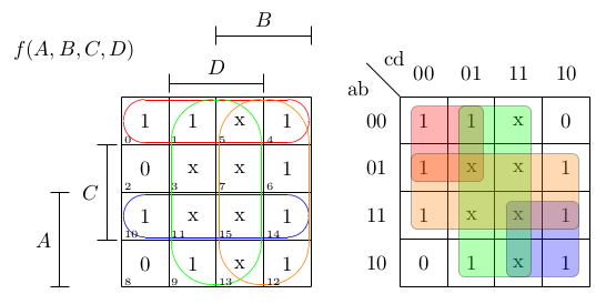
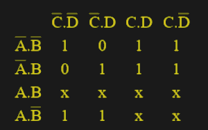
But how would we figure out a minimum in a more complex example? For instance, suppose you have a four-digit number and want to drive a seven-segment LED. Segment a, for example, is the top bar of the figure 8 that forms the display. It should be on for inputs 0, 2, 3, 5, 6, 7, 8, and 9. Then, you need to do this for six other segments. Hard to see exactly how to decode that, right?
Methods
Before computers would do it for you, there were two common methods to resolve things like this without resorting to brute force. The most notable of these is the Karnaugh or K map. These are great for a small number of inputs. Let’s go back to the two-bit number. Our K map looks like this one.
Each of these four cells containing a zero or one represents a single AND gate with A and B set as shown (that is, if A or B are true or false). The number in the cell is the output in that state. If you don’t care about an output given a certain state of inputs, you can put an X in that square and treat them the same as a 1 if you want to (but you don’t have to). By the way, these maps were made using the very useful K map solver you can find online.
Next, you circle all the 1’s that are next to each other in a rectangle including any that wrap around the edges. When you have a bunch of ones clustered together, you can wipe out the variables that change from 0 to 1 in the group.
In this case, the 1’s cover both A and A’, so we can easily see the answer is Y=B. Of course, we knew that already, but you can figure it out easily using a map like this, even if you don’t already know the answer.
For a map this small, you don’t have many options, but the number of 1s (or Xs) in an implicant — a group — must be a power of two. So you can draw a rectangle around two cells or four, but not three.
Bigger, My My…
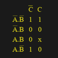
Note that the values of A and B only change by one bit in adjacent cells. So, a 3-variable K map looks like this is the one adjacent. Note that the left-hand column reading from top to bottom goes 00, 01, 11, 10. So, only one bit changes at a time (like a grey code).
In this case, the prime implicants — the parts that matter — are A’B’ and B’C’. That’s because the top row strikes the C input when AB=00 and the top left 1 and the bottom left 1 join to cancel out A.
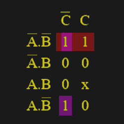
Every rectangular grouping that covers a power of two cells is a prime implicant. Sometimes, a group will cover terms that other groups will also cover. In that case, that group is not an essential prime implicant but, rather, a redundant prime implicant. But if even one square only belongs to a group, then that group is an essential prime implicant and will have a role in the final result. Sometimes, you’ll have several prime implicants that cover each other so that you can pick one or the other, and it doesn’t matter which one. Those are known as selective prime implicants.
As you can see below, once you have four bits, the K map gets large. Beyond 4 bits, it is usually impractical without switching how you draw the map. Remember the 7-segment decoder example? Here is the K map for segment A of a decoder that accepts numbers from 0 to 9. Note the Xs for numbers larger than 9. If you draw circles around the groupings of 1s, you can develop the formula: Y=C+A +B’D’+BD. That’s much easier than trying to do it without a K map. The C is due to the right-hand columns (remember to include the Xs when it helps you). The A term is due to the bottom two rows. The other two terms pick up the stray 1’s not covered by those two groups. Of course, to design an entire decoder, you’d need six more K maps, one for each segment.
It is also possible to group the 0s instead of the 1s and obtain a product of sums. The process is similar but you use the 0’s and not the 1’s.
The real challenge is when you want to go beyond four bits. For that, you often go to a table-like format known as the Quine McCluskey method. Or just use a computer. We won’t judge.
Of course, if you want to make complex digital designs, you need a clock. But you can still use maps where you need combinatorial logic in a synchronous design. We mentioned you can make anything out of AND, OR, and NOT. But you can get those gates using a multiplexer or even a relay, which is, after all, just a mechanical multiplexer. Come to think of it, you can make logic gates out of darn near anything.
Banner image by [Kit Ostrihon], demonstrating multidimensional K-maps
Thumbnail image: “K-map 6,8,9,10,11,12,13,14 anti-race” by [Cburnett]


Okay, it’s kindof hilarious you start off by saying “you can build everything you need for combinatorial logic with just those three components” and promptly show how only 2 of the 3 are needed: it’s like the AND and OR gates are there facing off Highlander-style: “there can be only one!” while the NOT gate’s like “whoever wins, you still need me.”
“Then came logic devices, which would eventually become FPGAs.”
The first programmable logic devices came before small-scale ICs, because *memory* is a programmable logic device. PALs/GALs were just PROMs with a few registers tacked on. There are old appnotes for FPGAs which suggest using block RAMs as “very wide logic functions” (there used to be an optimization pass that looked for this, if memory seves) because “memory as programmable logic” kindof encouraged it.
You can make a NOT gate from a NOR gate.
You really only need NOR or NAND gates. From either of those two, you can make all the others.
the apollo guidance computer is pretty much made entirely out of 3 input nor gates.
to take that further, you can make a NOR from some NANDs (4), so really you only ‘need’ just NAND — a ‘universal gate’ in classical logic. (the wiring is three nands as inverters on the inputs and the output of a nand, which will net result in a nor).
NOR is also a ‘universal gate’, where you can synthesize all logic from it alone, and it may be preferred in some implementations.
Yes, but the article only mentioned AND/OR/NOT. If you’re lucky enough to have a logical design where NAND/NOR are fundamental (which thankfully it is for transistor-based logic) you’re golden.
If you read a bit further down, it says exactly that….
PALs/GALs are *not* just a “PROM with tacked registers”.
A 20L8 PAL calculating parity on 19 input pins would require a 512Kbit ROM, not something readily available when PALs were invented.
PALs were based on “product terms” which were wide AND gates with input for both a signal and its inverted form, and you could disconnect unused lines. output pins used 1 or more of these “product terms” which were OR-ed to produce the final output. You could also share common product terms between outputs.
(Just google for the PAL 16R8 datasheet for example)
Some architectures used a variable number of product terms per output pin, so you would put the less complex equations on the output pins with less product terms and the more complex equations on the outputs with more product terms
Sigh, I need to put “basically” more often.
I really meant in terms of the *silicon*, not in terms of the logic. If you look at a PAL/PLA/GAL die it basically looks like a PROM with a bit tacked on. It can do more because of that “bit” part, but the silicon difference between the AND/OR planes and a PROM/ROM isn’t large.
If you look at an FPGA die, though, it’s like “this looks absolutely nothing like memory whatsoever” and that’s because they’re really very, very different devices. There are still use cases for CPLDs where they outperform FPGAs, and that’s why it’s annoying that they’re practically obsolete (and why it’s frustrating when Lattice calls a chip that’s an FPGA a CPLD). I’ve actually got a small hoard of CoolRunner IIs, but it’s a bit scary to me that they’ll be gone in a small number of years.
One of my colleagues was surprised to find out that an FPGA had a 15 ns in-out propagation time for what was fundamentally an 8-input arbitrary logic function: but that’s the cost of a large interconnect fabric – put stuff in the wrong locations and suddenly your super-fast FPGA becomes super-slow.
Here’s the thing. When you “well, actually” a post, someone can “well, actually” right back at you…
Oh, that wasn’t intended to be a correction! Basic memory gets excluded from programmable logic history often.
Boolean algebra solvers focus on “fundamental” (sum of products, etc.) terms, which map to PALs/CPLDs perfectly because of their memory-based history: wide input logic functions.
When you get to FPGAs, though, since they’re LUT-based, that doesn’t make sense anymore, because it’s more minimizing the number of logic levels and total LUT count. Even redundant terms don’t always have to be removed.
Of course modern FPGAs have become so huge that it doesn’t matter that the tools aren’t particularly good, unless you’re crazy and run them up near Fmax with heavy usage (which, sadly, I do).
Sorry, to clarify, what I was pointing out was that it’s actually a bit frustrating that the “old digital design titans tools” (which Al does a great job introducing!) are so focused on sum-of-product/product-of-sum forms, which, by this point, are practically obsolete in programmable logic devices.
I keep wondering if there’s some equivalent or fancy way of thinking about things for certain FPGA architectures, and there really isn’t.
The Universal NAND gate is a bit of a cheat. you actually need :
Invert a logic assertion
Amplify a logic assertion for fan-out
The and/or function. (non-symmetrical logic, not an xor or such)
The NAND gate that we all talk about is all three at once.
(It was great how k-maps were easy on the P.E. EE exam.)
No. NAND gate is only two transistor with a common pull-up resistor. It has only one more transistor than NOT gate.
NANDs rule!
If you want to learn how Seymour Cray and Steve Chen designed the Cray-1 and Cray X-MP using pretty much just boolean logic, this is a good video.
https://www.youtube.com/watch?v=yeFHQ1efhc0
It’s long, but you’ll learn a TON!
Thanks for linking that fascinating video. I think the history of logic design tools doesn’t get the attention it deserves.
*Real* greybeards know what a “bridging term” is, when you need them, and what happens if you omit one.
In my case the loss would have been three months and the equivalent of several years salary. Fortunately the omission was caught by a design verification check using a “transport” digital simulator (Tegas) rather than the “inertial” digital simulator (HiLo) that had been used during implementation
When I first started at Kodak I was told they never design using asynchronous circuits. I did.
Every input into a microprocessor is an asynchronous event. Even if you use the system clock. I never could figure out from the Intel and Motorola processor specs why the setup and hold times for inputs were longer than a clock cycle.
I often wonder if Meta Stability is still an issue. Or is the world ignoring that?
Lastly if you hit the brake, and the computer doesn’t record that you hit the brake; that does not mean that you did not hit the brakes. Just that the computer didn’t know it. Logic is a great subject to study.
Setup/hold for inputs being longer than a clock cycle just means they’re not enabled at that rate. For an MCU, for instance, they can’t be sampled at that rate anyway due to the instruction cycle time.
Metastability-hardened FFs in modern processes typically resolve in small fractions of a nanosecond nowadays. You can actually measure it in FPGAs since the clock modifiers/delays can move things by ~picoseconds at a time.
It actually can be a pain in the neck because you used to *use* metastability to detect a data valid window just by sampling and looking for bit errors. But if your sample adjust is coarse now (like ~100 ps!) you jump *right across* the bit errors and into another data valid window. Which means to detect the errors you need to double sample or know the incoming bit pattern.
I think this article comes from a good perspective. Binary tables are important, so it is great to introduce varying approaches. The right toolset is the one you can repeat and understand on a design level. All else follows.
It’s all just a little bit of history repeating…
If you understand Karnaugh maps you understand the need for undefined behavior in C and C++
Can you explain that in simple terms, because I definitely can’t understand it!
Yeah, I learned to program in Assembly Language (AUTOCODER) IN 1965, and did a lot of assembly on different systems for years after that. Back then we could “Desk Check” our code to make sure it ran right. Flowcharts were the approved tool, but the real efficiency came from using decision tables. Today, programming Arduino and other controllers, decision tables are one of my best tools.
Look up some of the cool books from the ’60s on Decision Tables and expand your basic understanding of what this article is about.
I recently took (and passed!) the PE electronics, controls, and communications exam; digital logic and k-maps in particular were a sizeable chunk of my studying and ended up being a few exam questions.
They got me on one question though regarding boolean simplification methods – the correct answer was the Quine McCluskey Method, which my studies apparently didn’t cover but it was too strange of a name for me to not look into after the exam.
Wow, that triggered some unexpected flashbacks from “Logic I”…
Also what was perhaps my first idea for a T-shirt:
“I’m just a don’t care in the Karnaugh Map of Life”
To give you an idea of how long ago that was, when we mis-wired a chip in the lab and released the magic smoke we called them “Chernobyl Chips.”
A very well-done article; perhaps more emphasis should have been placed on one of the most powerful tools available for logic minimization–De Morgan’s Laws;
more commonly known as De Morgan’s Theorem. Very simply, in plain English—
not (X and Y) = (not X) or (not Y), and
not (X or Y) = (not X) and (not Y).
Or, in Boolean algebraic format—
(X • Y)’ = X’ + Y’
(X+Y)’ = X’ • Y’
De Morgan’s Theorem can be expanded to any number of variables…
De Morgan’s theorem formula for 3 variables is
(X∙Y∙Z)’ = X’+Y’+Z’
and (X+Y+Z)’ = X’∙Y’∙Z’.
De Morgan’s theorem formula for 4 variables is
(W∙X∙Y∙Z)’ = W’+X’+Y’+Z’
and (W+X+Y+Z)’ =W’∙X∙’Y∙’Z’ .
…and so on.
———————————————
p.s.–
“…Suppose you wanted to determine whether a two-bit binary number is odd or even. Yes, yes, there is an easy way to do that, but assume you don’t know that yet…”
The “…easy way…” was never revealed. Here it is (but you probably already knew this): simply look at the LSB of the number, no matter the size of the binary number. “0” = “even”; a “1” means the number is odd.
By posting DeMorgan’s theorem, you may have denied Mr. Williams the next article he had planned on digital logic!
B^)
As long as there are those who think that the ‘old stuff’–the absolute basics–of design doesn’t matter any more (and there is somewhat a current of that mind-set running through these comments), he’s not going to be at any loss for material.
I tell my students that there’s one word to describe those people who fully understand the value and the absolute necessity of learning and understanding the basics of design–
“boss”.
@Al Williams said, “After all, you can do everything you want with just AND, OR, and NOT gates. Bonus points if you have an XOR gate, but you can build everything you need for combinatorial logic with just those three components.”
You just need one type of gate to build anything, a NOR or a NAND. See here:
Universal Logic Gates
https://en.wikipedia.org/wiki/Logic_gate#Universal_logic_gates
Charles Sanders Peirce (during 1880–1881) showed that NOR gates alone (or alternatively NAND gates alone) can be used to reproduce the functions of all the other logic gates, but his work on it was unpublished until 1933. The first published proof was by Henry M. Sheffer in 1913, so the NAND logical operation is sometimes called Sheffer stroke; the logical NOR is sometimes called Peirce’s arrow. Consequently, these gates are sometimes called universal logic gates.
> How can you do everything with a NOR gate? Easy if you don’t mind spending gates. Obviously, if I need a NOR gate, I’m done. If I need an OR gate, I just feed the….
> Bigger, My My…
Was that a Propellorheads reference thrown in? Kudos if so.
I may have bigger for him…
I *loved* the logic part of my college course, I could “de’Morganise” stuff in my head for all the coursework and more but it was such a long time ago and I just haven’t needed those skills until I started thinking about building myself a 6502 machine recently so this article is real timely.
I have a masochistic idea of building all the ‘glue’ using those single gate SMT logic chips because using PALs/CPLDs just feels like cheating :)
I guess no 555 this time.
…depends on how one was raised.
The professor from whom most all digital logic design was learned was adamant regarding one’s logic designs / implementations being strictly digital, to the extent that inclusion of a monostable multivibrator in one’s design would guarantee an “F”. A ‘monostable’, being dependent on Rs and Cs for operation, is, at heart, an analog device.
An SE / NE 555 is not–strictly–a digital device. The use of comparators (forget the external Rs and Cs) guarantees that.
“Most all”? Why not simply say “most” or “almost all”?
Sigh … If the reality is accepted that all physical gates inevitably have some delay, it’s even possible to make a monostable with nothing but NAND gates.
Reminds me of the time I ‘broke’ the digital electronics course at uni. We had a task to design a circuit to produce a truth table using the minimum number of gates. I showed my result and instantly was told it was wrong as I hadn’t used sufficient gates. Showed the demonstrator that it works correctly and he was quite surprised that he’d been giving this class for how many years and nobody had come to my optimised solution. Guess I should have gone into design FPGAs…
I don’t normally make comments unless I feel like I have something to contribute but couldn’t help expressing gratitude for the great refresher! Thanks Al!
You guys had it easy with DTL and TTL. All we had were diodes.
Diodes?
Luxury!
Pah. Ferrites and two Ge transistors to implement several types of 3 input logic gates. No diodes needed (just as well, since they were expensive in 1959!)
Next lesson: divide by 10 using two transistors.
“…Next lesson: divide by 10 using two transistors.”
…plus what other components?
None?
Neon lamps?
Relays?
Diodes?
Pencil (graphite) lead…
Or—is this a rhetorical question / problem?
Two transistors, two diodes, three capacitors, four resistors. Same circuit can also do divide by 2 and divide by 5.
FFI see the schematics in the Tek 184 manual (and keep an eye out for the cartoon figures :) )
Never mind.
Two transistors form the basis of a flip-flop, which is a divide-by-10 circuit.
“There are only 10 types of people in the world: those who understand binary and those who don’t.” — Unknown.