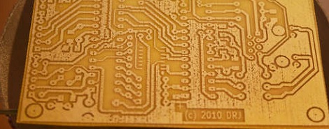
When it comes to making PCBs at home really quickly, there’s not much to improve upon with [Ryan]’s bodged up Epson printer that prints an etch mask directly on a piece of copper clad board.
Like most of the direct to copper PCB printer conversions we’ve covered ( 1, 2, 3 ), [Ryan]’s build relied on an Epson printer and Mis Pro yellow ink. The Mis Pro ink is one of the most etch-resistive substances that can be shot out of an inkjet printer, and Epson printer cartridges use a piezo pump that is perfect for squirting ink out on command.
After tearing the printer apart and lifting the print head a bit, [Ryan] needed a proper feed system to control where on the copper he was printing. He managed to make a board carrier out of a sheet of aluminum. By taping down the copper clad board, everything seems to work phenomenally.
After the break you can check out how fast [Ryan] can print out a fully etch-resisted PCB. It’s not improbable that he could produce a few dozen boards an hour; something our toner transfer PCB production method would kill for.
via makezine
[youtube=http://www.youtube.com/watch?v=Fpflg2KcORY&w=470]









“there’s not much to improve upon with [Ryan]‘s bodged up Epson printer”
As i can see from the pictures of the etched boards, there is a lot to improve. The boards look like Berlin after WW2! :D
I don’t know what settings were set in the printing setup, but you’ll get best results from setting quality to photo, thus making the printer spit out more ink. More ink means the areas will be covered way better.
Also, with our PCB printer (almost unmodified Epson photo R800 with special ink) we set paper type to “glossy photo paper”.
That was relating to the speed of the method, don’t pull it out of context :)
But I agree with you, there are many tiny holes, as it seems. You probably all know this: http://www.pabr.org/pcbprt/pcbprt.en.html those boards look somewhat better
His newer boards look much better:
http://www.instructables.com/id/Converting-an-Inkjet-Printer-to-Print-PCBs/step12/Etching-Revisited-October-24th-edit/
http://www.instructables.com/files/deriv/FBF/AZAO/GU1UZF0O/FBFAZAOGU1UZF0O.LARGE.jpg
“With special ink” would you please tell what brand of special ink you are using? A link to the site would be helpful. Thanks!
Cool! Have you played around with alignment for doing double sided?
Tweeks
What I really want to see is a build where the printer squirts out a ferric chloride solution (and whilst I’m dreaming it can print a solder mask later).
Not sure that’ll be happening any time soon though. I’ll stick to milling for home PCBs.
if you can print out a good solder masking material, solder seems to make a GREAT etchant resist (cant remember which etchant I was using when I confirmed that)
I use a pen plotter for my pcb’s two of the only inks I’v found that work are black sharpie ink and black Staedtler ink. SOMEWHERE its possable to get bulk bottles of the Staedtler ink, but from what I can tell, nobody in north america sells it (rather sell ya new pens) I’v tried writing Staedtler on this and I got no reply.
Agree with Nomad. Lots of room for improvement. The PC board looks pitted and an extra pass or the photo quality mode may give better results. Cool hack that has some room for improvement.
Personally, I want to get away from using chemicals. My next project is building a CNC PCB router.
A milled PCB is an alternative but certainly not easy. My limited experience with this highlights a few serious problems. As traces become thinner and pads smaller, I would bet on transfer methods having the upper hand.
1) Because typically conical bits are used, the depth of the cut must be precisely controlled. A bit too deep and the cut expands and eats adjoining traces. To high, and the bit stops cutting and skips across the surface. Since PCBs can have a slight bow, and it doesn’t take much, you really need a cutting tool that can track the board’s surface.
2) You need to spin the cutting tip like a deamon because the cutting circumference is so small. Burs along edges are not uncommon and sometimes the cutting force lifts thin traces right off the substrate.
Just my 2 cents. I’ve milled some simple boards on a cheap homemade CNC but never anything approaching what I could achieve with toner transfer. With proper equipment it probably becomes routine but never simple.
People have thought of that before. However, you might just order manufactured PCBs in this case. To go down to reliably doing QFP traces the machine needs to be very high quality, you need a high speed spindle and you will use a lot of cash for burr tips, even if you buy them used. I considered this as a professional solution for work, going with one of the commercial products, but it just didn’t make sense. The easiest thing with least hassle is CNC drilling of photo transfer etched PCBs. Any modern inkjet will spew out good enough templates on transparencies.
Saw this before, I thought on Hackaday.
The pitting was showing in that too. I wonder if running it through a second time after it dries would let you get a more solid covering.
Primera (I think) used to make thermal transfer printers (wax ink) which might work as well. Lower dpi but really nice results.
well why cant an epson print hot wax?
It’s a nice hack, no question. But I see no point in directly printing the PCBs. You can hardly do double sided, there are always quality issues, you have to go through all the heat gunning which will work out differently on different days and board sizes. Honestly, I just stick with transparencies printed by the inkjet in black and photo transfer. It works reliably and there is no hassle involved.
The Blue Press-n-Peel seems to yeilds better DIY results. And while a respect DIY PCB folks (I think everyone should at least etch one DIY board from scratch).. the costs have come so far down on professional grade, multi-layer PCB fabrication, I was able to have this 7×14″ pro grade board created for just $33 back in 2003!
http://theweeks.org/tmp/SHOW/2_b_demux-pop1-rear_l.jpg
I used the outfit called “Advanced Circuits”:
http://www.4pcb.com/
Freak’n amazing results.
Tweeks
Nice quote, illuminutty face.
@Steve:
You might be right about double sided. But that could be achieved by further development (zero coordinate etc)
And quality is an issue of ink. I would love to have such a printer. That would safe me a lotta money :-)
CHALLENGE ACCEPTED!
We should have a race to really see just how fast these different methods can produce a PCB.
No need to all be in the same place either, just as long as the video we submit is un-cut and you start the timer when you press PRINT on the computer, and stop it when the board is completely etched. Alternatively you could stop it when the board is ready to be etched, but I believe that’s not completely fair because the board is not finished and there are many different methods for etching.
The design should be 100% SMT as well, so we don’t have to mess with drilling (you CNC guys can enter as well, just don’t drill any holes). The design should have a wide range of trace widths and package types, but not necessarily be a functional design.
When we are done, the PCBs should be SCANNED and submitted for the second half of the scoring. Opens and shorts count against your final score.
All machines used to make the PCB besides the computer with PCB ready to print must be turned on AFTER the start of the video.
You supply your own materials.
Hackaday staff will judge the competition and finalize the rules.
If you want in, reply here below…
This could be a thing.
Awexome… how can we make this happen? I’m game for the toner transfer method.
I’m prolly the only one with an XY plotter, iirc it takes me about 3 to 5 mins to get a board ready for etching, my primary limitation is line with of 25 thou. on a good day, I CAN sneak a trace between .1″ pins. I can do soic. do we make our own designs?
I would say there has to be one set of design files for all, probably a set of Native EagleCAD and Gerbers, or just Gerbers… I’m thinking the “design” would be a series of different trace widths (100 mils, 50 mils, 25 mils, 12 mils, 8 mils) and SMT package types (SOIC, TQFP, QFN, MSOP, SOT-23, 0402, 0603, 0805, 1206, etc..). It would be nice if it actually DID something so after our 3 minutes of hard work (chuckles) we could then spend time building it up to see if it lives. However, making a real circuit that everyone is interested in might be a challenge in itself. At least a copper “eye chart” is something we can all agree seems fitting for this comparison if fabrication techniques, and then it’s a nice piece of wall art. Maybe the design looks like the Hackaday logo, but done in traces and chips ;-) Couldn’t be too hard to sprinkle some LEDs all over it as well… hmmm….
noise. my garage is directly below the neighbours apartment. not cnc suitable, atleast not in the middle of the night when i want to make adjustments to a board.
I have 10cmx15cm pcb circuit designed by protus software, i need to print it out as single layer pcb.
would you please advice me which printer is siutable for this jop? and which ink i have to use?
shortlly i need your recomendatins and advice to know which printer i should buy??
I have 10cmx15cm pcb circuit designed by protus software, i need to print it out as single layer pcb.
would you please advice me which printer is siutable for this jop? and which ink i have to use?
shortlly i need your recomendatins and advice to know which printer i should buy??
No need to wreck a decent but old printer. TheEpson Stylus Photo R-range of printers has a thickness adjustable CD Print facility with a decent size width to print small PCB’s . Together with the MISPRO ink’s it should be easy to make quality PCB’s.
Hi,
I tried using MISPRO yellow ink. The printing perfect but during etching (sodium presulphate solution 20g to 100ml water) simple peel off the ink from the board. I tried different heating from 100C untill 250C degree but the same problem. I think the problem is the adhesion between the board and the ink.
Can somebody tell me what sould be the problem?
Thank You
Ferenc
You have to bake the ink before etching at sufficient time and heat. For MISPRO yellow, according to members of the Homebrew_PCBs site where this was developed, is about 230C or 446F for about 3 minutes. The ink should darken a bit, and the surface of the copper will turn purplish.
http://techref.massmind.org/techref/pcb/etch/directinkjetresist.htm
Above distilled from these two Yahoogroups:
https://groups.yahoo.com/neo/groups/Homebrew_PCBs/info
https://groups.yahoo.com/neo/groups/Inkjet_PCB_Construction/info
Check out the photo on the homepage of the second Yahoogroup, it was done with inkjet resist.
Not long ago I tried my hand at MOKO http://www.mokotechnology.com/, a company located in China Shenzhen delivering PCB services for from prototype, production to turn-key demands. Up to now, all things go well.