Unlike microcontroller projects, projects involving FPGAs cannot yet claim to rely on a mature open-source toolchain. Each FPGA will, at some point, need to be configured with a proprietary bitstream produced from a closed source synthesis tool. This lack of a full FPGA toolchain to take your project from Verilog-or-VHDL to an uploadable bitstream is due to many reasons. First, writing such a “compiler” is complicated. It involves intimate knowledge of the resources available on the FPGA that can assimilate the functionality of the intended design. Second, the entire synthesis procedure is closed-source, a “secret sauce” of sorts for each FPGA vendor.
In response, [Alex] and [Clifford] have taken the first step towards an open-source toolchain for one FPGA; they’ve reverse-engineered the bitstream of Latttice Semiconductor’s iCE40 FPGA. The duo didn’t just pick the iCE40 on a whim. This choice was deliberately because that FPGA is available on a development board for a mere $22 so that others could follow in their footsteps without breaking the bank.
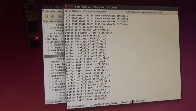
In the video below, [Clifford] demos the functionality of this new tool by synthesizing a design from Verilog to a bitstream and then back from a bitstream to Verilog. Given this feature, a staggering amount of work has been done towards developing a polished open-source toolchain for this particular FGPA.
To snag a copy of the latest code, have a look at its documentation page.


I was thinking you could download libaes1024.zip from and them turn it into a FPGA that implements AES1024
You can… sort of. It just involves porting to Verilog (if you can’t find a Verilog implementation) and fitting it into the appropriate FPGA. Probably would be a bit rough in an ICE40 though ;)
“This lack of a full FPGA toolchain to take your project from Verilog-or-VHDL to an uploadable bitstream is due to many reasons.”
Yep and they aren’t technical issues. Instead it’s companies like Xilinx sending C&D notices if anyone does something they don’t like. I wouldn’t be surprised if this guy’s page and all his information about it disappears a few days.
Thanks, downloaded the source instead of making a bookmark :-)
I wanted to buy a laptop recently, but I don’t like windows very much. Then I remembered that microsoft used to give refund’s if you don’t want their software on your newly bought hardware. Did some browsing and found out that the refunds where between 10 an about 130+ dollars (us, au, & other currencies).
The most remarkable was however that I stumbled upon a suspicious amount of dead links in that niche of web.
This is awseome work! I love that they went the whole hog and made a tool that spits out RTL Verilog. I don’t know Lattice parts very well but I’ll be giving this a shot. It presents all sorts of opportunities.
FPGA manufacturers tend to keep their sauce secret, not just from each other but also to protect themselves from liability in case you were to inadvertently damage a part e.g by internally shorting the power rails or having several line drivers fighting each other or getting some PLL filter magic coefficients wrong. Xilinx produced a java based library several years ago to enable you to do direct placement and routing yourself, but it still relied on their tools for final synthesis and I don’t think it’s a thing any more.
Incidentally, this bitstream hackery was also done on Xilinx 3000(?) series FPGAs by some guys in the late 90s. ISTR they got bought off by Xilinx.
The Xilinx Java tool was called JBits, and they canned it with Virtex II >10 years ago! It enabled you to select logic functions for individual tiles and wire them up manually.
Mucking around in the bitstream on Xilinx devices is pretty easy: if you want to know where various logic bits are initialized, or various block RAMs are initialized, you can just ask the bitstream generator (bitgen) to tell you. That part’s not exactly that complicated.
there really isn’t much “magic” happening in an FPGA. Most of the “secret sauce” is really routing resources, and some hard-ip configuration. What they really want to keep secret is things like interconnect delay, and how the synthesis tool chooses paths, etc.
Reverse engineering bitstreams in the past is what vendors were really worried about. That way, people could clone the FPGA, or worse, make it into a much cheaper ASIC, or even a MCU given the right resources. No suprise that the H1k has internal NVM for the configuration bitstream.
The work done is excellent, but it doesn’t implement a synthesis tool, which is what really is missing in the Linux world.
Sure Synopsys-DesignCompiler runs on Linux, but few people have the millions of dollars required to purchase a license, let alone all the libraries and other tools required.
Clarification: The cloning part isn’t so much an issue for the someone making Chinese FPGA chip, but more towards protections for their end customer’s IP. FPGA has been marketed as a secured chip that OEM can put their magical secret sauce that their competitors would have a hard time imitate and improve upon i.e. DRM. So having a bitstream to reconstruct back to HDL form is bad news there.
To make your own clone of A*/L*/Q*/X* FPGA is pretty much an expensive operation as the vendors themselves are often using one of the 2-3 bleeding edge fabs. The chip fabs are often using FPGA as test beds – where else do you have a customer with deep pocket already lined up to make very large array of tidy blocks of logic for their bleeding edge process?
This research isn’t going to help much with reverse engineering a user design though. On most FPGAs you have the option of encrypting with a NV key stored on the die, and even if that’s not available you can get “secure” SPI flash with on board RNG into which you can store some critical initialisation vectors. Security of user designs against copying is a nut that has been cracked.
Far more interesting is the ability to improve the place and route tools you are forced to use, which have traditionally been buggy, slow or in the very recent instance, hobbled.
> The work done is excellent, but it doesn’t implement a synthesis tool
Clifford also wrote a synthesis tool, yosys, which takes Verilog through technology mapping:
http://www.clifford.at/yosys/
At this point the only thing missing is place and route.
I’m not aware of any “Alex” working on this project. Mathias did all the reverse engineering work, as mentioned on the documentation page.
There is another reason why this is interesting. Modern CPUs have a microcode update facility. The micro-code is generally implemented either as a ROM/RAM combination, or possibly a PLA/FPGA like resource inside the CPU.
Most vendors don’t encrypt their microcode, since they don’t have even block diagrams of the mcirocode storage/decode unit.
Just an interesting thought.
Does any hobbyist actually use the iCE40?
I have the USB stick development board, but I haven’t tried it out yet. It looks like a nice product with small and very cheap packages available, some with integrated flash for bit stream storage which is nice.
The reason ice40 was a good target was not so much to do with availability – many are available on cheap devboards – more that it’s an extremely simple device, without many of the more complex blocks like PLLs, multipliers, memory and funky I/O standards that most other FPGAs have.
Hate to nit pick, but ice40 appears to have 4k ram blocks, LVDS (inputs) and some PLLs. The project in the OP mentions they haven’t reversed the configuration bits for the memory arrays or the I/O blocks yet, but the address/data routing is identical to that of the configurable logic.
I hope this motivates further action in this area .. its definitely an arena ripe for the plucking. Imagine if we could gain access to the walled-garden of many, many microcoded dies in fabrication today .. it would perhaps kick off a new era of freedom, if we were – for example – truly able to understand how some of our cheaper CPU’s were constructed. Heck, even the expensive ones too ..