Serial Peripheral Interface (SPI) is not really a protocol, but more of a general idea. It’s the bare-minimum way to transfer a lot of data between two chips as quickly as possible, and for that reason alone, it’s one of my favorites. But that doesn’t mean that everything is hugs and daffodils. Even despite SPI’s simplicity, there are still a few ways that things can go wrong.
In the previous article in this series, inspired by actual reader questions, I looked into troubleshooting asynchronous serial connections. Now that you’ve got that working, it’s time to step up to debugging your SPI bus! After a brief overview of the system, we’ll get into how to diagnose SPI, and how to fix it.
What is SPI?
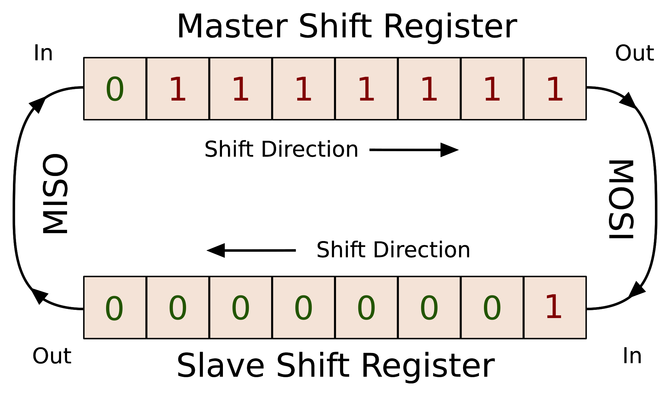 The core idea of SPI is that each device has a shift-register that it can use to send or receive a byte of data. These two shift registers are connected together in a ring, the output of one going to the input of the other and vice-versa. One device, the master, controls the common clock signal that makes sure that each register shifts one bit in just exactly as the other is shifting one bit out (and vice-versa). It’s hard to get simpler than that.
It’s this simplicity that makes SPI fast. While asynchronous serial communications can run in the hundred-of-thousands of bits per second, SPI is usually good for ten megabits per second or more. You often see asynchronous serial between man and machine, because people are fairly slow. But between machine and machine, it’s going to be SPI or I2C (and that’s the next article).
 Turning this pair of shift registers into a full-blown data bus involves a couple more wires, so let’s look into that now, and cover the labelling of these wires as we go. The master controls the clock (CLK or SCK) line, that’s shared among all of the devices on the bus. Instead of a simple ring as drawn above, the master’s shift register is effectively in a ring with each of the slave devices, and the lines making up this ring are labelled MISO (“master-in, slave-out”) and MOSI (“master-out, slave-in”) depending on the direction of data flow.
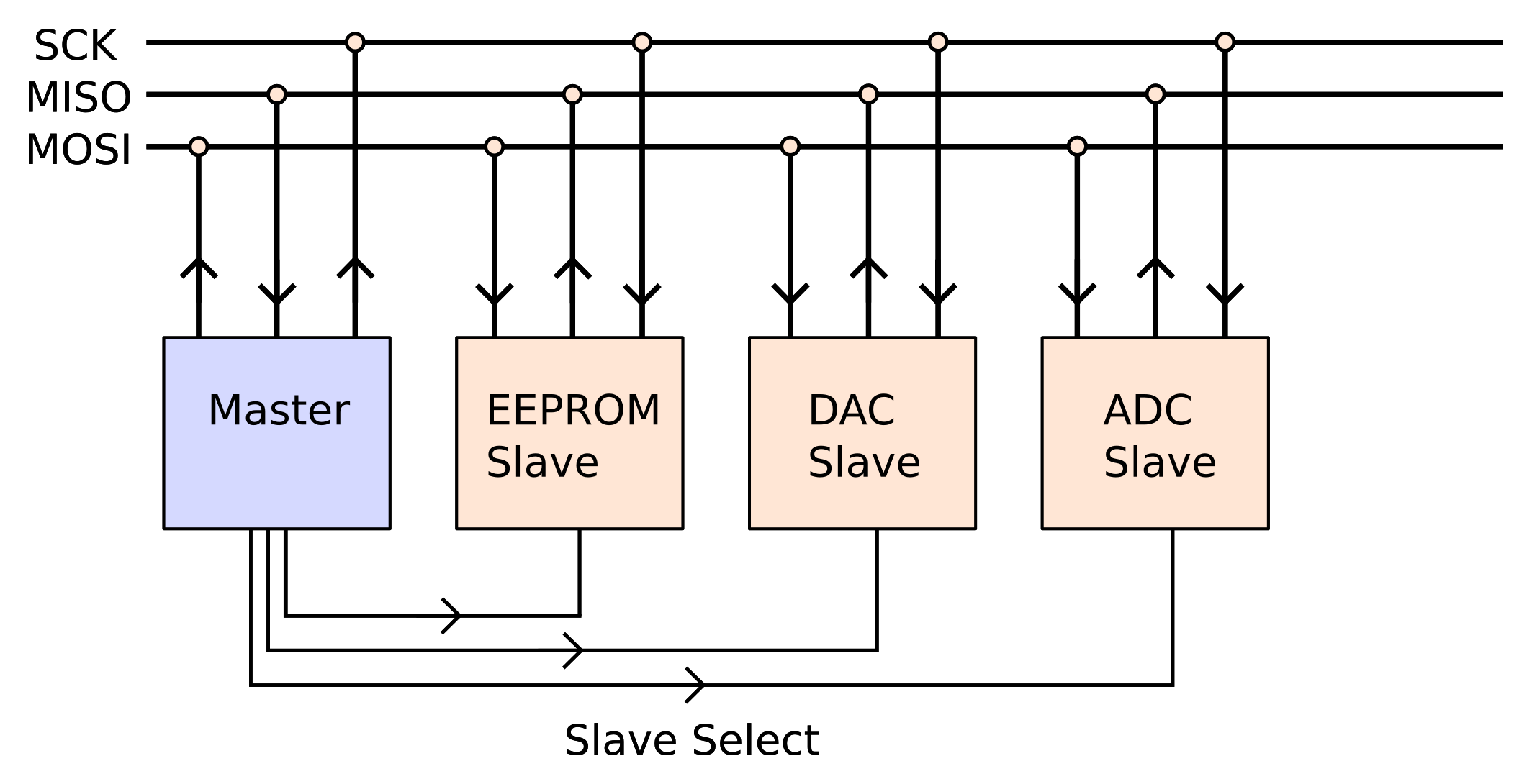
Since all of the rings are shared, each slave has an additional dedicated line that tells it when to attach and detach from the bus. That is, each slave has a slave-select (SS or sometimes called chip-select CS) line, and when it’s high, the slave disconnects its MISO line, and ignores what comes in over MOSI. When the individual SS line is pulled low, the slave engages. Note that the master is responsible for keeping one and only one SS line active low at any given time.
Typical SPI Communication:
- The master pulls the slave’s personal slave-select line low, at which point the slave wakes up, starts listening, and connects to the MISO line. Depending on the phase (covered in detail just below) both chips may also set up their first bit of output.
- The master sends the first clock pulse and the first bit of data moves from master to slave (along MOSI) and from slave to master (along MISO).
- The master keeps cycling the clock, bits are traded, and after eight bits, both sides read in the received data and queue up the next byte for transmission.
- After a number of bytes are traded this way, the master again drives the SS line high and the slave disengages.
 Here’s a concrete transaction, between a microcontroller master and a 25LC256 SPI EEPROM. First, the master drops the CS line. Then it starts clocking in the command — in this case binary
 00000011, the read command. The next two bytes from the master are the read address. All the while, the slave has been holding its MISO line low, returning zeros. After receiving the read address, the slave starts sending back its data. In the case of this EEPROM, it will keep sending sequential bytes until the master stops clocking and raises the CS line, ending the transaction.
Looks easy enough when it’s working!
Phase and Polarity
Here’s the number-one problem with SPI lines, and the first place to look if you’re troubleshooting. If you look carefully at the traces above, you’ll notice that both chips pushed their data out on the MISO/MOSI lines at the falling edge of a clock cycle. What you can’t see, but you could probably guess, is that they both read in on the rising edge — right in the middle of a clock period.
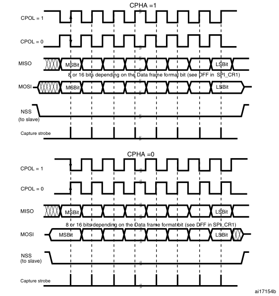
The choice of which edge to read data on, as well as whether the clock signal idles high or low, presents two binary variables that can change from one chip to the next, giving us four different “versions” of SPI. The idle state of the clock signal is called clock polarity, and it’s easy to explain. A clock that idles high has a polarity = 1, and vice-versa.
Unfortunately, if you like thinking about when in the clock cycle the chip reads the data, the industry decided to latch on to another aspect of the transmission which maps to the same thing: the phase. Phase describes whether the data is going to be read on the first clock transition (phase = 0) or the second (phase = 1). If the clock idles low (polarity = 0) the first transition is going to be upward, so a system that samples on the upswing will have phase = 0. If the clock idled high, however, the first transition is necessarily down, so a system that samples on the upswing will have phase = 1 — sampling on the second transition. My head hurts even writing it out.
Here’s how I cope. First, I look at when the data is sampled. If data is sampled on the upwards clock edge, the phase equals the polarity, otherwise it’s the opposite. A read-on-rising-edge is 0,0 or 1,1. And since the polarity makes sense, it’s easy to pick between the two. If it idles low, you have 0,0.
| Sample on Rising Edge | Sample on Falling Edge | |
|---|---|---|
|
Clock Idles Low |
Phase: 0 Polarity: 0 |
Phase: 1 Polarity: 0 |
|
Clock Idles High |
Phase: 1 Polarity: 1 |
Phase: 0 Polarity: 1 |
Most everyone uses 0,0 or 1,1: data is read on the upward-going edge, and reset on the downswing. Some devices are picky about which of these two you’re using, while others aren’t. For instance, the Microchip 25LCxxx series of SPI memories samples on the upswing and doesn’t care at all about how the clock idles. That’s my kind of chip.
Where this ends up, if you’re too lazy to read the datasheet or if you’re reverse-engineering, is a four-way choice. If it’s your only variable, it’s not hard to brute-force. Most chips have a status register or a chip ID. Set the phase and polarity on your microcontroller, and send the command to read the known data out of the slave device, and verify the answer. If phase and polarity is your only problem, you’ll have the right configuration in a jiffy. If your problems run deeper, you’ll have to move on. And if you don’t have the datasheet, you’ve got four times the work to do, so get this right if you can.
Speed
Because SPI is clocked, and the slave-select line delimits a conversation, there’s not much that can go wrong in syncronizing two devices. Not much, except when the master talks too fast for the slave to follow. The good news? This is easy to debug.
For debugging purposes, there’s nothing to lose by going slow. Nearly every chip that can handle SPI data at 10 MHz can handle it at 100 kHz as well. (If you know exceptions, post up in the comments!) On the other hand, due to all sorts of real-world issues with voltages propagating from one side of a wire to another and the chip’s ability to push current into the wire to overcome its parasitic capacitance, the maximum speed at which your system can run is variable. For really high SPI speeds (say, 100 MHz and above?) your system design may be the limiting factor.
So test it. Start slowly and work your way up until you start noticing errors, and then back off. I’ve never had problems with short lines at 10 MHz, but you never know. The images here are from the EEPROM, which is rated for 10 MHz, soldered on a sketchy breakout board and connected through a bunch of 20 cm (8″) DuPont cables. You can see it meeting (just barely) the requirements at 9 MHz, but lagging at 18 MHz. At 35 MHz, it can’t even switch the line fast enough to produce any signal at all.


More Clocking!
If you’re sending a command to an SPI slave and expecting an answer that never comes, double-check that the master is continuing to toggle the clock until the slave is done.
This can be counter-intuitive, but remember how SPI works — it’s a ring of shift-registers. To get data out of the slave’s shift register and into the master (and vice-versa) there needs to be clock pulses. The master is responsible for sending this clock, and knowing how long it needs to toggle the clock.
For the EEPROM I’m using as a demo, it will continue to spit out sequential bytes until the clock stops. Most memories work this way. But other devices, like temperature sensors, will often only return a byte or two. If you keep clocking after that, they often return all zeros. When the slave must return a variable-length packet, it can either transmit the expected length first, or send bytes terminated with an end-of-data marker. This is all higher-layer stuff. I just want you to remember that if you want data back from the slave, you have to give it a clock.
Bus Problems
So far, I’ve been considering what can go wrong for each individual slave on the bus. If you add more devices to the bus (each with their own CS line, but sharing CLK, MISO, and MOSI) things can get hairy. In principle, all devices have tri-state drivers for their output lines so that they can pull it high or low, and detach when necessary. In principle, devices never speak (transmit on the MISO line) except when they’re spoken to (their CS is dropped low by the master). In theory, everything works out just fine.
Switching Phase and Polarity
Remember the four possible combinations of phase and polarity? That goes for each device on your bus. Keeping track of which device is being spoken to and setting a couple configuration bits isn’t hard, it’s just that you can’t forget to do it. Demonstrate to yourself that you can talk to all of the devices already on the bus each time you add a new one. And if you ever change modes, start writing the code you’ll need to change back.
Bad Actors
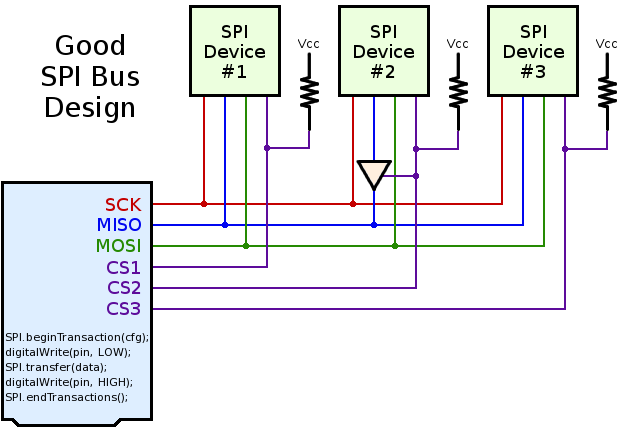 The master can only address one slave at a time. If you’re getting garbage across MISO, make sure that only one CS line is asserted low at a time. If that’s the case, it’s conceivable that one of the slaves is misbehaving. You can try unplugging devices one at a time until you find the culprit.
[Paul Stoffregen] was having trouble with SPI compatibility on the Arduino platform due to slaves that weren’t releasing the MISO line. His solution is to add a tri-state buffer chip to the offending device, and tie the tri-state line to the chip’s CS line, so that it can never tie down the MOSI line except when it’s being used. This is a great solution to the problem.
Open Collectors
While some slaves drive the MISO line too much, others drive it too little. In particular some slave devices may fail to pull up the MISO line, scrimping on one transistor and only pulling the line down. If this is the case, the MISO line might need a pull-up resistor attached. Again, this is non-standard, but is for instance true of SD-MMC memory cards that use the SPI-like interface. By adding pull-up resistors to the MISO line, you can pretend that it’s SPI.
The Test
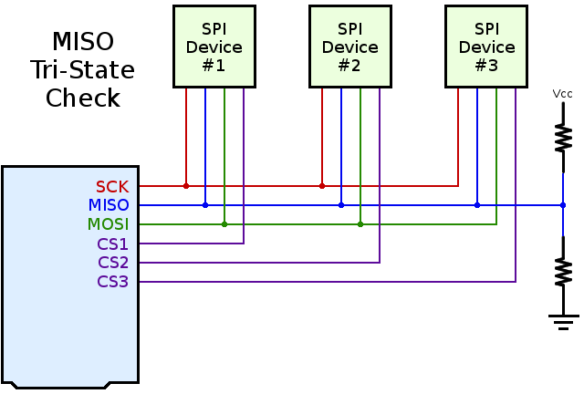
To test for MISO-line problems, both bad actors and open collectors, you can temporarily attach a pair of (say) 100 kOhm resistors to the line, one to VCC and one to GND, serving as a weak bias to the mid-rail voltage. Put all the CS lines high, so the slaves should detach from the bus. If any chip is failing to tri-state, you’ll see the line pulled up or down when it should be resting in the middle. Those are the bad actors. Now run the bus. If a chip can only pull the line down, you’ll see what looks like valid data, but it will vary between mid-rail and GND instead of VCC and GND. There’s your open collectors.
Initialization
Not unrelated, what happens when the microcontroller that serves as your SPI bus master is just booting up? The voltage levels on the SPI bus (and the CS lines) are floating — essentially random. The clock line might pick up power-line signals and oscillate at 50 or 60 Hz, and some chips might start talking to each other, or get into strange states, before the micro asserts control.
For this reason, some people advocate (weak) pullup resistors on the CS lines, so that even before the microcontroller is up and running, all of the SPI devices are de-selected. You might think that this is a power-waster, but since the CS lines idle high anyway, the resistors only conduct when a chip is selected. I’ve never had trouble bringing SPI chips up from power-down myself, but give it a shot if you experience odd behavior on startup.
Summary
Debugging a broken SPI bus isn’t actually that hard. Since the lines are unambiguously named (CLK, MISO, MOSI) you don’t have to think very hard when wiring the circuit up, but double-check your wiring anyway. Most of the time, you’ll have the configured phase and polarity incorrectly, which can be solved with an oscilloscope and a peek into the datasheet. After that, it might be a speed issue, which is easily fixed by just slowing down until it works and troubleshooting from there. You are clocking the slave’s data out, right?
If you’ve got a bus of SPI devices, you can troubleshoot each one individually, as long as they’re behaving. Pulling the MISO line weakly to mid-rail and seeing if it stays there can verify that they are. And don’t forget to switch modes between slaves if you need to.
If you’re using an SD-MMC card, or if all else fails, or if you’re just somehow superstitious, you can try adding pull-up resistors to various lines to stabilize them during power-up or for some other magical reasons. SPI should be a bus with push-pull drivers on all sides, so you shouldn’t need pull-ups. But then again, your bus should also be working.
As always, I’d love to hear your SPI debugging tips, tricks, and horror stories!


Good article, I like it.
Another idea for article: I2C bus. I think there is even more things to go wrong, like misbehaving slave holding SDA, causing bus contention (by the way, do you know how to get out of this? I battled this in one of my projects), proper pull-up resistor values, fast and ultra-fast I2C modes (being partially incompatible with good old I2C), SMBus which is actually more-less compatible, but not static. And don’t get me started about multimaster I2C.
Honestly, I hate I2C and use it where really needed. It takes a lot of work to make properly and that’s why it usually isn’t done properly. What is the last time you’ve seen timeouts and its handling in I2C master libraries?
I2C is up next. I’m looking forward to it as well. I generally go for SPI just because I find I2C a pain to work with.
I2C slave mode for 8-bit PICs is almost impossible. Microchip screwed up their only app note on the subject. Master mode on the other hand works like a charm. Clearly Microchip dislikes I2C slavery…
I2C slave mode has never “worked like a charm” on any mcu in my experience. There are inevitably small delays while the processor determines whether to read or write and how to reply. This can be handled with clock stretching at the cost of data rate on your bus. Being able to add more devices to a bus with minimal hw development is the cool part of I2C, and you can’t reliably use many other devices on a bus that is clogged by one mcu.
Hey YOU!
Quit using my name unless you are making a point about Brian!
And since I got called out for only making fun of Brian and never contributing anything…
If you don’t need the extra speed, the only thing bad I have to say about I2C is that level shifting and isolating are much more of a pain than with SPI.
I suggest you both switch to DC instead of arguing about AC.
When both datasheet and app note lies, you are screwed, Implementation example is wrong, datasheet is wrong, and only random post on forum points to the solution. So after a year I have semi-working slave, that locks out the MCU whenever CTMU acquisition is interrupted by I2C request. So I’ll have to switch from “as fast as possible” sequence to “take your time, interrupts ar disabled anyway” model. Also XC8 sucks monkey balls when it comes to adhering to ANSI C standard. I tested that with other project that used standard implementation of linear feedback shift register for PRNG…
I absolutely hate it when engineers start blaming anyone they can find as long as it’s not their fault they couldn’t get something working. It’s the app note, or the software library, or the development board, ignoring the fact that there are probably thousands and thousands of those things out in the wild begin used by people who know what they are doing every day. It’s one thing to have an actual bug, and when that happens companies document that stuff in an errata. It’s a very very safe bet that your Adruino/PIC LED flasher project is not doing something so exotic that you uncovered a previously unknown bug.
The only way to get out of this is to segment your I2C bus into smaller sections to isolate the problem. If you don’t have multiple I2C master on your uC, an I2C MUX can be used. I2C MUX also help to lower the capacitance on a heavily load bus by breaking it up so you can run the bus at a faster speed.
> misbehaving slave holding SDA, causing bus contention
Any “bus” topology suffers from this. Should SPI device go nuts, communication is going to be disrupted for all bus members. That’s inherent drawback of any bus topology.
I2C also got some advantages:
1) Multi-master. It is difficult to use SPI for “communication of equals”, where either device could start communication. I.e. there’re no multi-master setups for SPI, not by standard/obvious means at least. One could extend it to handle roles switching but it not going to be something standard or expected. OTOH I2C allows multi-master setups.
2) I2C is much better at defining bus states. No this phases/idle states crap, idle state and phases things are defined in specs. If someone violates it, they do not talk i2C, but something else. As simple as that.
3) Btw, there is SMBus, which is derived from I2C in its core and extended to handle System Management things better. It specifies “bus reset” procedure, partially handling what you’ve scared of. Upon certain bus condition devices MUST release bus and reset internal states related to bus handling if they are SMBus-compatible. Obviously, older I2C devices not aware of SMBus do not have this knowledge, so it is half-way there. But lo, SPI entirely missing this procedure and who told you nothing could go wrong with SPI devices?
4) In I2C slaves could delay communication a bit. Requirement to output reply right after command received could be difficult to implement in some cases. What if one needs plenty of processing before answer is known?! I2C deals with it to some degree. though mentioned caveats apply.
As disadvantage, I2C is slow. Nearly all devices talk 100kHz mode. But only some devices are talking faster 400kHz mode. There is even faster mode specified, but it is obvious even less devices understand it.
Another nasty thing about I2C it is open-drain/open-collector thing. This could be a bit nasty in terms of power usage. It requires pull-ups. It wastes power to heat them when lines are held in low state. So once there is intense date exchange it wastes plenty of power for no good reason. Not a big deal on mostly idle bus, but suxx otherwise.
Use I2C isolators or hubs for devices you’re not sure are going to hang up the bus. Isolators have timers that cut off devices on the individual ports (usually 4 per chip) but do nothing for addressing. Hubs actually have addresses and are also called I2C bus extenders or address extenders because of that. Sitting at 0x50 or 0x70 and having 2, 3 or 4 ports that can be turned on or off. TI PCA9518 or ISO1540 come to mind.
If you clock the SPI bus too slow for a ADC, conversion errors cans creep in – check the specs on an ADC for it’s minimum clock speed.
I once had to interface an ADS7843. We had some serious nonlinear distortions on large touch screens until someone tried to use a slower SPI clock.
Bits, not bytes. SPI can transfer any number of bits in a unit. Case in point would be the common Nokia-style LCDs, which use 9 bits (1 for data/command flag, and 8 for payload)
Another fancy thing is the fact JTAG is mostly some specific subflavor of SPI. Also, SD cards are required to be able to operate in “SPI mode” where one could use microcontroller to talk to card (multi-bit modes are using different protocol and most uCs do not have suitable hardware aka full-fledged mmc/sd controller, larger socs do). For MMC cards SPI mode is optional but most MMC cards actually implement it, just like SD cards.
Elliot
As ever nice description and helpful tips but you only mention 8 bit SPI. Personally I have experience of 16 and 32 bit buses meeting all the other SPI requirements. Further, I have met three systems which are supposedly using SPI buses but which have no slave select lines and an arbitrary bit length. These are great fun to debug until you get hold of the loop length particularly if the micro clocks everything continually.
The trick here is simply to go back to basics and check the chip specs and assuming they are all SPI compatible chips or shift registers, not micros, simply add the bits up. I have just finished working with a system that had fifteen, eight bit registers cascaded on a so called SPI bus; it works like a dream once you understand what is going on.
Frank
Good points Frank and Alphatek — you’re absolutely right about bits vs bytes. 9 bits is just perverse. Alphatek, how did you work around it? Bit-bang one and use the hardware for eight? Or just do it manual all the way?
In comparison, the multiples of 8-bits are pretty pleasant to deal with, no? The memory chip in the example, for instance, takes a 15-bit address with one bit of padding so that it fits nicely into two bytes. Just remember which byte goes first, and all’s well.
In one case, pure software bitbang (8051), in another bitbang+hw (attiny), and on another, got the hardware design to cope with arbitrary bits 2-32.
I wholeheartedly agree that i2c is evil incarnate, especially as a slave!
I’m my experience the only thing standard about SPI is that is usually 3 or 4 pins and one of them clock. Especially things like ADCs seem to do all kinds of things like, strange number of bits, 3 wire with opposite clock polarity for reads or half bit turn around, data lines doubling as busy indicators many of them making DMA or hardware chipselect useless
I had to do 17-bit reads and writes to configure a sensor. And the spi engine would insist on whole bytes. This would leave the shift register on the device partway shifted. So after each transaction, I’d have to initiate a bunch of throwaway reads until the device’s register was back around to the first bit.
That’s what you get when you buy $20000 sensors, I guess.
I used a micro so it was easy build a pair of circular buffers to act as the shift registers and go. The length is then almost irrelevant, the input static bytes/bits and output circular on the transmit, the opposite for the receive. The only caution is not to read the response at the wrong time or you get a corrupt answer. The data in the recieve circular buffer is only complete between frames.
As for I2C I’ve had no problems using PICs and NXP parts it just works once configured correctly. The biggest problem is if you need lots of address range, extra lines or chips are necessary. My problem there was the mapping of a custom TFT to the internal registers of the driver and nothing to do with the chips! Let a draughtsman choose the interconnect layout and the glass will look great but your code will be dreadful.
Because my products depend on SPI, I have an approach/avoidance reaction every time a new Raspberry Pi or RPi OS update is announced. I’m always worried they’ve done something new to screw up the SPI clock, or if they’ve changed the timing between the end of a transfer and the rising edge of chip select. Both of these things have bit me in the past since I use the SPI peripheral on a PIC microprocessor.
Hmm, have RPi spiggots failed to learn to use Linux’s own SPI framework to do it right and rather keeping reinventing that damn wheel more and more? I’m using differend SBCs and do not really get why SPI should be an issue. Though RPi aren’t great engineers and always manage to screw everything up, be it SoC boot (GPU booting CPU? What the hell is that?) or power management (or to be exact utter lack of it, while even $5 Allwinner and Rockchip SoCs could do real dynamic voltage-frequency scaling!). No wonder they could screw SPI up either.
Can you say something about SPI Mode 0,0 and Mode 1,1, that is often mentioned in datasheets? What does it mean?
https://en.wikipedia.org/wiki/Serial_Peripheral_Interface_Bus#Clock_polarity_and_phase
https://en.wikipedia.org/wiki/Serial_Peripheral_Interface_Bus#Mode_numbers
Phase, Polarity. There’s a headlined section in the article, and I even made a table that breaks it down for you.
BTW those clock looks horrible – lots of ringing and undershoots. Plenty of newbie mistakes: using ground strap on scope probes for high speed signals, loose wires without series terminations.
You should have series termination (probably around 100 ohms) and or slow down the slew rate (if your chip supports it) if you are dealing with loose wires. Going with ribbon cables with alternating ground returns would help quite a bit.
I suspect grounding the scope probes is all that’s required…
LOL, did you see the picture of the “test setup”? It’s totally worst-case scenario! It’s the fastest thing I could lash up using wires on-hand to get some scope shots for the article. There’s no way you’d ever do anything that horrid in practice. Dupont cables flopping all around in the breeze and all.
You criticize the grounding? It’s worse than you think! I didn’t just use the ground strap — I used a jumper wire upstream of the ground strap. The ground path to the scope is like 20cm long with a sketchy joint in the middle.
My point was actually, given how horrid it all was, that it works just fine up to (spec) 10 MHz. SPI is, signal-wise, reasonably forgiving at fairly decent speeds.
In an earlier draft I talked about slowing down edges, but it didn’t make the final cut. Best/simplest solution, short of the chip doing it for you, is an RC filter right next to the output pin. That way you avoid dumping power into a grounded resistor as you would with termination, _and_ you limit the frequencies on the data lines, which cleans up radiation problems. (“Best” is IMO, natch.)
But because termination of SPI lines is not really needed in most projects (or maybe just in my experience!) I left that section out. To be discussed in comments. :)
Why termination instead of slew-rate limiting?
FPGAs often do run the SPI bus fast enough for termination to be an issue. In my experience adding a series 100R/100p RC snubber (play with the values) at the receiving end does pretty well to suppress overshoot.
For some real fun, select the wrong clock phase by mistake. The result is often a system that works intermittently or mostly works but is unusually sensitive to signal quality.
It is a really good example that illustrates what fail looks like, in a high-speed digital system.
High-speed digital integrity requires attention to the driver devices, transmission lines, impedance control and termination, and all sorts of other stuff which is basically bringing in all the same sorts of challenges and skills one encounters in RF design. None of this stuff is specifically unique to SPI.
Once I had occasion to work with an SPI slave (which was, under the hood, a microcontroller itself) that would reliably receive and transmit at 1MHz _unless_ the previous command you’d sent it was one of a select few that caused it to miss bytes here and there if you sent two in a row without stretching the clock.
Also, beware: some devices maintain a notion of transactions that must begin with a falling edge of /CS and end with a rising edge of /CS, while others you can just tie /CS low and send multiple back-to-back commands if you really need to save a pin. If you ever go out of sync with no way to signal a new transaction you can be up a creek (or at least need to reset the slave device entirely).
The maxrefdes24 “alameda” PMOD board with 4x isolated voltage/current 16 bit outputs is like this.
There are 5 different chips on the one SPI bus, and four of them are the output buffer / monitor chips which have to be all in the one 64 bit long transaction, because the chips are wired in a proprietary daisy chain configuration so they all expose just one CS.
“If the clock idled low, however, the first transition is necessarily down,” low should be high.
It’s a good article.
I’d prefer such titled articles not leave anything out though.
Eg: Most significant bit first vs the opposite : although I can’t bring to mind a specific device that goes LSB first.
I think the MSB convention (bit big endian) is so the data on the oscilloscope screen reads left-to-right how you would write it.
Another point is that SPI in particular tend to emit a lot of noise – especially where you use it between boards, which is becoming more popular to do what with the rash of convenient readily available PMOD’s.
I’ve yet to actually implement it, but I’ve found wirewrap with twisted pairs and differential logic signalling good for suppressing such noise – even if the devices don’t support differential signalling.
If you have a thevenin equivalent R nearby the slave device’s non-complement CLK input – what’s important for EMI is that the pair as a whole’s current doesn’t fluctuate with the signal. This is easy from an FPGA where you have nearby optional outputs designed to generate a complement of the signal right at the pin and in exact phase with the (on chip) clock.
It’s not a bad idea while you’re at it to make sure there are at least anti-reflection series resistors at the signal source too.
Even without the slave chip “using” the clock complement signal (since it would just be hitting the equivalent load resistor) this will massively reduce EMI emissions since it will carry the current for the pair whenever the clock line is low, so that the return path had only got a constant current source and therefore no ground bounce.
The final thing to do is to pass all wires through a suppression ferrite to absorb common mode noise – make sure you pick one made from ferrite with a lot of loss in the VHF.
Of course, if you’re connecting between FPGA’s, SPI with proper differential logic signals are even better – you can very easily hit half gigabit transfer rates, so long as you don’t mind the extra pair for the clock.
This makes particular sense if you need to split a design between chips – very long shift registers are very “cheap” routing and register cost wise on FPGA’s.
Oh, and it’s fairly easy to make pretty good twisted pair (or twisted triple: to accomodate the return current if it’s the only link between two boards) with 30AWG wire, a vice and a drill.
If it’s important, you can even hook up a signal gen and oscilloscope at the “vice” end, and put an impedance matching SMD resistor at the drill end, and then run the drill just past where the reflections die. (It’ll unwind a bit when released, of course).
This is a good way to get the right twist rate to use for the wire you have: there are calculators, but experiment is best.
For twisted triple, remember that it’s supposed to be two transmission lines that are that just happen to be close by : you don’t care about the actual differential line impedance, you want each impedance to the return to not reflect.
In that case you should put the scope on one line, and make sure you’re sending well-synchronised complementary edges down the other.
In fact this is kinda true of all differential digital : the impedance that actually matters most is the single-side to ground one. What’s confusing is that differential impedance matters for analog differential signals. But digital ones are really two signals which have the same length (and thus timing), and whose currents sum over time to some DC value. They still both need the third connection for the return path to ground – unless they’re transformer-coupled like Ethernet uses.
(But once you start with the transformer coupling, you can’t do SPI anymore, since then you need to whiten the data to ensure the transformers don’t end up saturating when too many like bits get sent in a row. You can still do this fairly easily, with 8/10b encoding – and this also allows you to ditch the clock connection as well, but it’s no longer as simple to set up and diagnose as SPI.
All of the above assumes no multidrop busses, of course: but you can have as many bus segments as you have PMOD’s on an FPGA, each “SPI bus master” can be just a single-page module of Verilog.
You bit-bang the CS lines with your soft-core, but use the SPI master to handle the actual send and receive shift registers.
Something that’s tripped me up with SPI, when reading multiple values quickly from a high res ADC I also needed to monitor a “busy pin” that indicated when the ADC was ready to be read. For this reason the hardware feature on my MPU (ARM STM32F4) couldn’t be used to simple read 256, etc values from my ADC. Instead I had to read one value, wait and repeat. I really wish their hardware feature supported this fairly common challange. On the same thread, the hardware feature didn’t support 18bit transactions. Only 8 and 16bit. So I was forced to do three 8bit reads and process the data :/ Their new F7 chip supports 24bit reads, but still no 18bit love. That kindof flexibility at the hardware feature level would be really nice in the future. Presuming 18bit ADCs are here to stay.
One other problem that may arise is SPI peripherals that don’t behave nicely. Some years ago, I worked with the AD7714 programmable ADC. This chip kept the shift register active at all times, and used the rising edge of chip select to transfer the shift register contents into the internal data register.
The controller board(s) I was using had the SPI chip select lines multiplexed with other functions (keypad, LCD) because of limited I/O capacity, so scanning the keypad or sending certain characters to the LCD would cause a momentary chip select with no data clocked on the SPI lines. This had no effect on any other SPI peripheral chip we were using, but it caused the last data sent to any other SPI peripheral to update the configuration for the AD7714 with incorrect data.
For such edge cases you need a configurable serial bus the FRDM K82F has flexio – https://mcuoneclipse.com/tag/flexio/ , this lets you implement your own bus protocols.
Is there any advantage of different SPI modes(the CPOL/CPHA) ? Or these modes are there because there was 4 different ways ?
It’s so refreshing to find an article where the writer is truly trying to make themselves understood – rather than showing off their superior knowledge! Well done on this SPI piece – a lot of very useful information, clearly explained.
Thanks Elliot!
Hi,
I am using two types of EEPROMs. First one is 25LC320E and 25LC32AE. First one have less clock(2MHz) supported and second one have clock (5MHz) supported at 2.5 – 5.5V chip. With my first one my sw working(read and write successful) but when i replace with second one this is not happening. Can you suggest any issue regarding.
I refered both the data sheets and everything seems to be correct.
I have interfaced ICM-20649 motion sensor with nrf52832 with SPI communication, not able to make communication.
I am having very hard time and stuck on this problem since weeks, so i can see correct clock frequency on the oscilloscope but no response from MISO and MOSI. Flash memory and motion sensor are connected to common SPI bus with dedicated CS to each slave, as mentioned in the above post that master can communicate with one slave at a time, i put CS pin of flash memory high and CS pin of motion sensor low explicitly in the code, still i got no response from MOSI.
However i am getting register value who_am_i(Register to indicate to user which device is being accessed) as defined in datasheet, make me to assume that there is some communication between mcu and peripheral. I even desoldered flash memory to eliminate the doubt of multiple SPI connection.
At this point of time i am not even able to say where the problem lies whether in hardware or firmware.
I would be share my story after solving my problem, meanwhile if anyone can suggest anything is appreciated.
Anybody out there have any luck talking to an ADT7320 temperature sensor? We have one device mounted on a 4 layer board and can communicate with the device on the board without difficulty at a 500 kHz clock rate but when using the same code to try to talk to a second device connected to the mail board with a 12″ long 6 conductor flex cable we get either no MISO activity at all or what appears to be MISO activity resulting from really fast false clocks. We have tried putting a 180 ohm series resistor in line with the SCLK and MOSI lines adjacent to the micro and reducing the clock speed to 100 kHz with no improvement in communication. The same 7320 device connected directly to the main board communicates reliably but will not work at all when connected with the 12″ cable.
Pretty much ready to forget about using the 7320 anywhere we cannot provide a good ground plane under the device and associated SPI lines. Why would anyone build a temperature sensor that you cannot talk to at the end of a cable?
Have you attached an oscilloscope to the SPI signals on the temp sensor to check the data integrity?
– Ideally ground/signal on twisted pairs for critical signals such as SCK (grounded at both sides). This helps to minimize changes in the impedance. This is higher than a transmission line PCB, but as long as you match it, you’ll be okay. Use series termination at source for impedance matching.
e.g. 30R source driver + 68R = 100R
– Don’t forget decoupling cap (0.1uF) and bulk cap (10uF or higher) for your sensor AT the chip.
– Edge rate (i.e. slew rate) is what’s affect reflection. Some uP (such as ARM) have programmable slew rate can help a lot. Otherwise the only way you can do is to increase the series termination at the driver.
Changing clock speeds have little effects on driver slew rate (hence signal quality) unless it is a timing margin issue.
In SPI, ‘clock polarity’ (CPOL) and ‘clock phase’ (CPHA). is quite confusing… It’s not clear even in diagram…can you clarify…
I am using 2 spi slaves and one slave has a long cable of 1m and other with a normal jumper wire. both of them works with small cables, the problem comes when i switch to long cable for my sensor. i use same spi lines. any idea how to make it work? with one spi, long cable it works. both together it wont.
Your third diagram that is SPI timing diagram, is it SPI MODE 0 ?
The 4 modes are represented on this diagram, look at CPOL and CPHA which are the polarity and the phase, respectively.
Great article which explains how SPI works very well and some nice tips at the end, thanks. I’ll definitely need the 2x100K test at one point. One thing that caused me problems in the past was using an ESP32 as an SPI Slave with another MCU as the Master. For some reason the ESP’s pins are not tristate by default with a stock chip, so it clogged the bus during the first tests when the ESP’s firmware was not yet loaded. When there is only one MCU on the bus this should not be a problem, but be careful when you try to interface other MCUs as slaves on your SPI bus.
> If the clock idled low, however, the first transition is necessarily down, so …
This should read “If the clock idled high, …”.
Hey thanks! Fixed. Wonder how many people have been scratching their heads for the last four years…
Hello Elliot, the most detailed article i have read about the SPI working till date. thank you very much, I have one question in case all the slave devices, say 4 slave devices, put up a CRC error message at the same time, how to prove that the master was the culprit in this case? or there can be any other factors contributing?
Hi first of all thank you for the information.I was working for SPI and I am facing issues with modes and lsb msb bits.
for mode 3 only lsb bit and msb bit first are working fine but in case of others means in case 0 msb wont work for case 1 and case 2 garbages are coming (These changes are for loopback communication were i am using same data sending from master and receiving to master)
Another issue I was facing was on first iteration(from slave to master transmission) no data is transmitting but clock is generating and after first iteration data are transmitting successfully
So please help me with this matter
I had a strange problem using one of those very inexpensive eight channel 24 megahertz logic analysers that you plug into a PC. I’m running two AD9833 signal generators from a Raspberry Pi 3 using the SPI bus. When everything was connected up, they wouldn’t work. But when the MOSI line was connected to only one of them, irrespective of which one was connected, the connected one worked fine.
It turned out that the logic analyser thing was injecting about a one volt 50 Hertz signal into the MOSI line, when I disconnected the logic analyser, it worked fine, but what’s peculiar is that it only screwed it up when both of them were connected together, not when only one was. That I haven’t been able to explain.
Do you have any ideas?
So far my only lesson from this is to use better logic analysers!
Thanks to this article for solving a problem I’ve been chasing for several hours. My first venture into sharing a SPI bus (Video chip & SD card). Turned out the SD card needed a tri state buffer on the MISO line.
>> Nearly every chip that can handle SPI data at 10 MHz can handle it at 100 kHz as well. (If you know exceptions, post up in the comments!)
Think I found one ADS1235… seems to have a very short hold time on the last bit of DOUT/MISO (th(SCDO2) >15ns, no max or typical given) For 2MHZ clock speeds and less on ESP32, this would give always ready the last bit as a one. For SPI clock at 10MHz it works. Similar results when probing with lower vs higher sample rates on Analogue discovery. Seems like slower SPI clocks have longer delays between falling edge and actual sampling of MISO, which result is sampling invalid data
Hi Elliot,
My name is Tony. I am a beginner on SPI.
I have 1 question about your SPI EEPROM read sequence in this article which is :
How the SPI master knows that data from EEPROM is available in order to clock and get it ? I meant the handshake protocol between Master and Slave for this regard.
Is it with timer or anything else ? as there is NO indication except the Slave places data on MISO signal.
Thank you for response.
Tony
Hi Elliot and everyone in this Forum,
I really appreciate your help answering my above question.
Thank you very much and have a great day.
Tony